Wiring structure for an integrated circuit

a wiring structure and integrated circuit technology, applied in the direction of electrical equipment, semiconductor devices, semiconductor/solid-state device details, etc., can solve the problems of increasing the width of the wire, reducing the wiring density, and compliing the manufacturing process,

Inactive Publication Date: 2003-12-16
RENESAS TECH CORP
View PDF4 Cites 17 Cited by
  • Summary
  • Abstract
  • Description
  • Claims
  • Application Information

AI Technical Summary

Problems solved by technology

For the purpose of reducing a resistance, which is required in ground / power-supply wiring, increase of a wire width W is effective as expected from the above-noted equation for the wire resistance R. However, increase of a wire width W has a non-negligible disadvantage of inviting decrease of wiring density.
However, to provide different wire thicknesses T for the signal wires 21 and the ground / power wires 22 would complicate a manufacturing process.
For this and other reasons, significant problems would be produced, and thus the method described above is not suitable for practical use.
In addition, increase of a coupling capacitance Cc causes a further disadvantage of canceling a noise margin between the signal wires.
As discussed above, increase of the wire thickness T for reduction of resistance causes increase of a coupling capacitance Cc with various significant problems.

Method used


Image

  • Wiring structure for an integrated circuit
  • Wiring structure for an integrated circuit
  • Wiring structure for an integrated circuit

Examples


first preferred embodiment

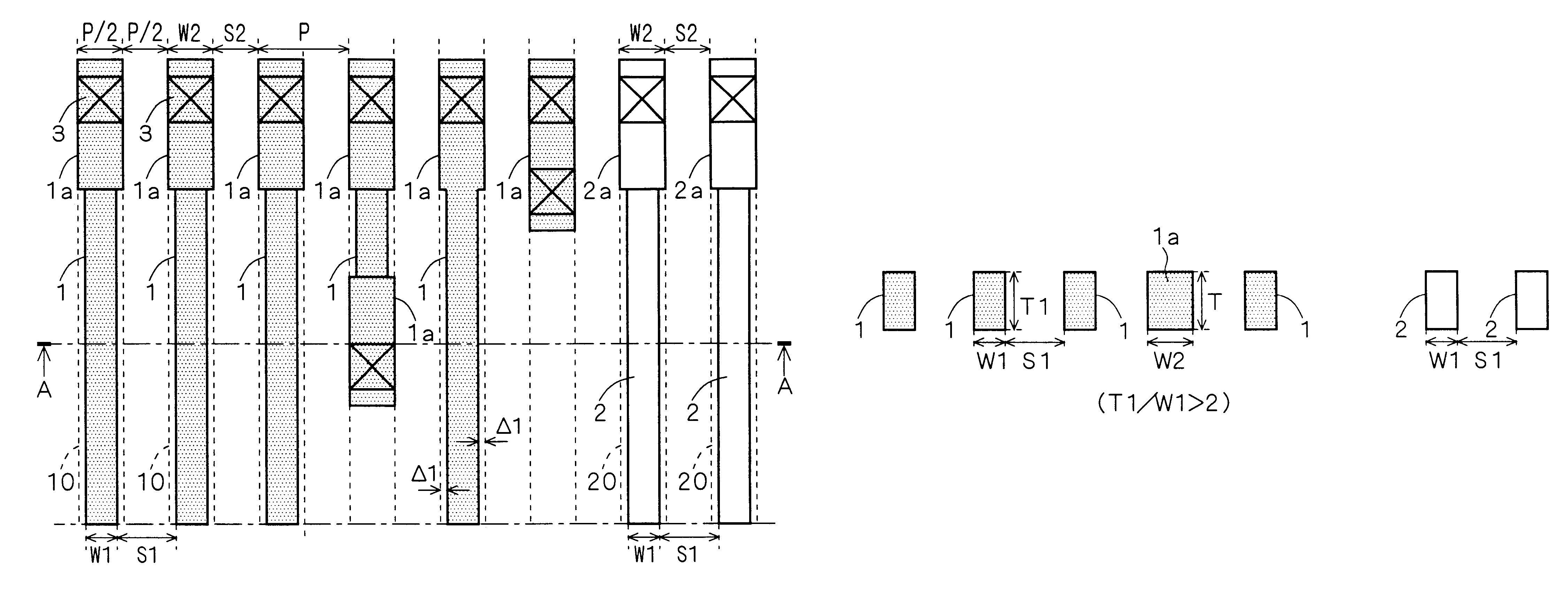
FIG. 1 is a plan view illustrating a wiring structure of an integrated circuit according to a first preferred embodiment of the present invention. FIG. 2 is a sectional view schematically showing a section of the structure of FIG. 1 taken along a line A--A of FIG. 1.

Referring to FIGS. 1 and 2, a plurality of signal wires 1 and a plurality of ground / power wires 2 are arranged. A wire width W of a main part, other than a via-hole neighboring region 1a, of each of the signal wires 1 is determined to be a wire width W1, and a wiring space S between the main parts of every two adjacent ones of the signal wires 1 is determined to be a wiring space S1. A wire width W of the via-hole neighboring region 1a of each of the signal wires 1 is determined to be a wire width W2 larger than W1, and a wiring space S between the via-hole neighboring regions 1a of every two adjacent ones of the signal wires 1 is determined to be a wiring space S2 smaller than S1. In an analogous manner thereto, a wire ...

second preferred embodiment

FIG. 9 is a plan view illustrating a wiring structure of an integrated circuit according to a second preferred embodiment of the present invention. FIG. 10 is a sectional view schematically showing a section of the structure of FIG. 9 taken along a line B--B of FIG. 9.

Referring to FIGS. 9 and 10, the plurality of signal wires 1 and a plurality of ground / power wires 4 are arranged. A wire width W of the main part, other than the via-hole neighboring region 1a, of each of the signal wires 1 is determined to be the wire width W1 (the minimum wire width), and a wiring space S between the main parts of every two adjacent ones of the signal wires 1 is determined to be the wiring space S1. A wire width W of the via-hole neighboring region 1a of each of the signal wires 1 is determined to be the wire width W2 larger than W1, and a wiring space S between the via-hole neighboring regions 1a of every two adjacent ones of the signal wires 1 is determined to be the wiring space S2 smaller than S...

third preferred embodiment

FIG. 12 is a plan view illustrating a wiring structure of an integrated circuit according to a third preferred embodiment of the present invention. FIG. 13 is a sectional view schematically showing a section of the structure of FIG. 12 taken along a line C--C of FIG. 12.

Referring to FIGS. 12 and 13, the plurality of signal wires 1 and the plurality of ground / power wires 4 are arranged. A wire width W of the main part, other than the via-hole neighboring region 1a and a wiring-space margin side 1b, of each of the signal wires 1 is determined to be the wire width W1, and a wiring space S between the main parts of every two adjacent ones of the signal wires 1 is determined to be the wiring space S1. A wire width W of the via-hole neighboring region 1a of each of the signal wires 1 is determined to be the wire width W2 larger than W1, and a wiring space S between the via-hole neighboring regions 1a of every two adjacent ones of the signal wires 1 is determined to be the wiring space S2 ...


PUM


Abstract

A wire width and a wiring space of each of signal wires 1 and ground / power wires 2 are determined to be a wire width W1 (the minimum wire width) and a wiring space S1, respectively. A wire width and a wiring space of the via-hole neighboring region 1a or 2a are determined to be a wire width W2 (>W1) and a wiring space S2 (<S1), respectively. The wire widths W1 and W2 and the wiring spaces S1 and S2 are respectively determined so as to maintain the minimum wiring pitch P. The wiring space S1 is determined also so as to satisfy {S1 / P>=0.6}. Further, the signal wires 1 and the ground / power wires 2 have the same wire thickness of a wire thickness T1 which allows an aspect ratio (T1 / W1) to be equal to, or higher than, 2.

Description

1. Field of the InventionThe present invention relates to a wiring structure of an integrated circuit which takes into account a resistance and a capacitance associated with an electric wire in the wiring structure.2. Description of the Background ArtWiring of an integrated circuit is broadly divided into two categories: (1) signal wiring for transmitting a signal or a clock; and (2) ground / power-supply wiring for providing a power supply potential or a ground potential.For (1) the signal wiring, it is important to reduce a delay time in signal transmission, which requires reduction of an RC delay time obtained based on a product of a wire resistance R and a wire capacitance C.On the other hand, for (2) the ground / power-supply wiring, it is important to reduce an IR drop of a (power-supply / ground) voltage, and thus it is preferable to reduce a wire resistance R, as generally known.In most cases, signal wiring is accomplished using a wire width W and a wiring space S which fit in a m...

Claims


Application Information

Patent Timeline
Patent Type & Authority Patents(United States)
IPC IPC(8): H01L23/52H01L23/528H01L21/82H01L21/822H01L21/3205H01L27/04
CPCH01L23/528H01L2924/0002H01L2924/00
Inventor OHSAKI, AKIHIKOFUJISAWA, MASAHIKOMORIMOTO, NOBORU
Owner RENESAS TECH CORP
Why Eureka
Try Eureka