However, as the number of devices on PCB's has increased and the sizes of the PCB's have decreased, it has become difficult to place these wires in such a small area.
This results in an incredible amount of congestion in a very small area.
In addition if there is a malfunction, it is very difficult to identify a single dysfunctional wire within the 4000 wires.
However if there is spacing between either board and the probes, the test signals may not be conducted or may be conducted and produce incorrect readings.
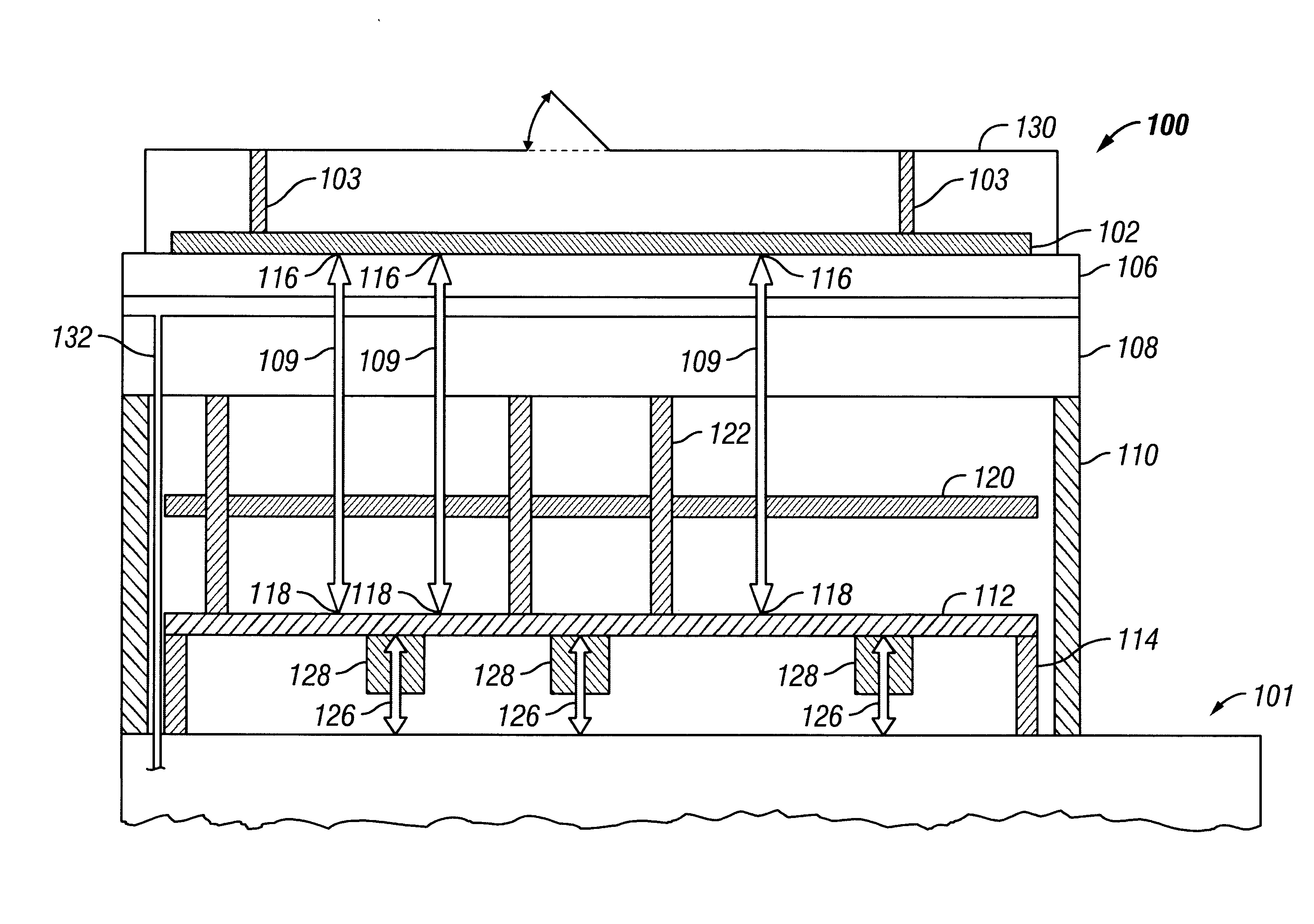
As a result of the foregoing configuration, a great deal of stress can build up in a fixture.
There may be non-uniformity or imbalance between the forces.
Probes may not be uniformly distributed in the fixture.
The non-uniform distribution of probes result in a non-uniform distribution of forces in the fixture and in the probe plate.
When the upward forces do not balance the downward forces the fixture and the probe plate may experience an imbalance in forces.
When the fixture and the probe plate experience an imbalance of upward and downward forces or alternatively, if the upward force is distributed in a different manner from the downward force, the probe plate, the board under test and the
wireless PCB may ultimately deflect, deform, and possibly fracture.
For example, a deflection of the probe plate, the
wireless PCB or the board under test may produce stress in the probes.
The stress may cause probe tips at the end of the probes, which contact the board under test and the wireless PCB to fracture.
The body of the probe itself may fracture.
Ultimately, the
stress conditions in the probes may result in a failure of a probe and as a result incorrect test readings or analysis may result.
In addition, the probes are contained and trapped within the configuration of the fixture; therefore the probe ends only displace a limited amount.
Therefore, unbalanced forces appear in the probe plate and both PCBs, as a result, the probe plate and the PCB's may deflect and deform.
Deflection of the probe plate and the PCB's ultimately may result in failures in testing.
In addition hairline
stress fractures in the PCB's may cause incorrect readings.
However, it would be hard to detect whether the incorrect reading were due to the probe plate deflection, a failure in a PCB, a device on the PCB, or a trace between devices on a PCB.
As a result, the forces resulting from a deflection of the board under test are borne by the bit in contact with the board under test and result in a downward force on the probe and the probe plate.
In addition, the forces resulting from a deflection of the wireless PCB are borne by the bit in contact with the wireless PCB and result in an upward force on the probe and the probe plate.
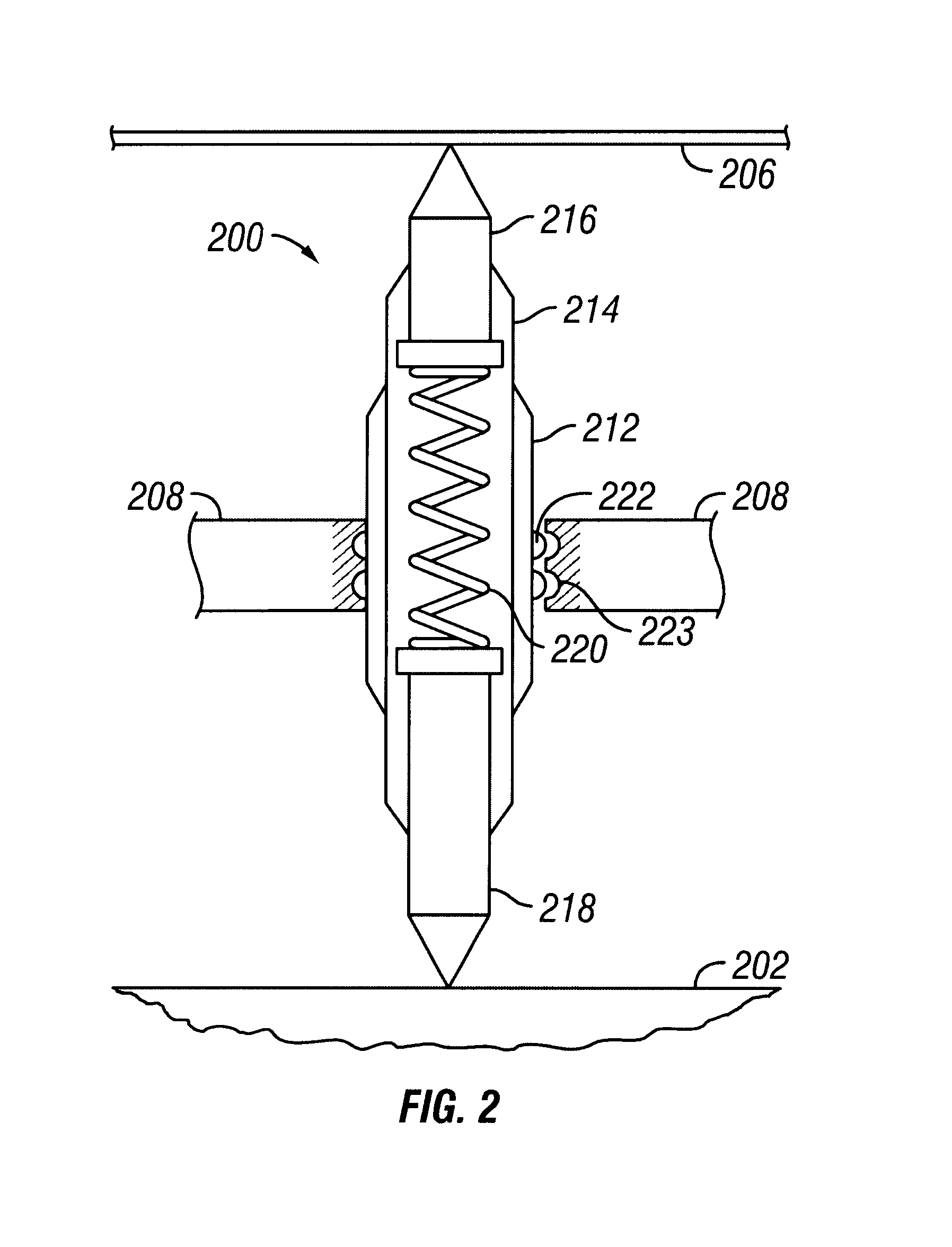
In addition, if these probes are allowed pivotal movement around their center axis, the probes may swing out of position and the bits may lose contact with pads when forces are applied.
Stresses in the probe plate resulting from forces transferred through the probes; result in deflections in the probe plate.
Deflections in the probe plate may result in the misalignment of one or multiple probes with the pads in the boards.
In addition, misalignments of the probes may result in structural failures in the probes.
Both the misalignment of the probes and the
structural failure of the probes may result in the incorrect reading of test signals.
Lastly, failure of the probe plate, such as hairline fracture or deformation,
impact the probes and as a result, it becomes very difficult to troubleshoot whether there is a problem with the probe plate, the contact of the probe to the board, a bad device on the board under test, or a bad trace on one of the PCBs.
As a result a significant imbalance of forces occur in the fixture.
As a result, once again, a significant imbalance of forces may occur in the fixture.
As mentioned earlier, the imbalance of forces, now caused by changes to the fixture configuration, may result in board deflection, probe misalignment and general fixture failure.

