Photomask producing method and apparatus and device manufacturing method

a technology of photomasks and manufacturing methods, applied in the direction of photo-taking processes, printing, instruments, etc., can solve the problems of increasing the amount of write data needed by a lithography system for producing a photomask, increasing the manufacturing cost of photomasks, and increasing the area of original photomasks needed for exposur

Inactive Publication Date: 2004-01-13
NIKON CORP
View PDF11 Cites 42 Cited by
  • Summary
  • Abstract
  • Description
  • Claims
  • Application Information

AI Technical Summary

Benefits of technology

It is a first object of the present invention to provide a photomask producing method which can form an original pattern within a short period of time.
Accordingly, as the reduced images of N sets of patterns of parent masks are transferred, overlapped one on another, the averaging effect reduces the effect of the writing errors of the lithography system and the distortion or the like of the projection optical system for performing reduction projection of patterns of parent masks.

Problems solved by technology

Because the areas of devices, such as recent LSIs, are getting larger, and the miniaturization scale and integration are constantly being improved, however, the original patterns of photomasks which are needed for exposure are becoming larger in area and becoming more miniaturized.
Because of these reticles, the amount of write data that is needed by a lithography system for producing a photomask becomes enormously large.
Such increased writing times are factor in raising the manufacturing cost for photomasks.
It is, however, difficult to keep performing complex correction with high precision and stability, and there has been a problem of drifting of the writing position during writing.
Writing may be interrupted to carry out calibration, which inconveniently makes the overall writing time longer.
When the miniaturization of pattern rules for semiconductor devices or the like advances further, therefore, the writing time for the original pattern of a single photomask will becomes too long, resulting in a variation in precision, so that the required writing precision may not be achieved.
Further, the amount of write data in a control computer is becoming so large that it is difficult to use the data in single writing.
As the laser beam lithography system also directly writes an original pattern, the amount of write data is becoming so large as to make data processing difficult and the writing time becomes considerably long so that the required writing precision may not be achieved due to drifting of the writing position or the like.
Although a predetermined pattern may be transferred on a substrate for a photomask by using an optical projection exposure apparatus at the time of producing the original pattern of that photomask, the accuracy of the original pattern gets lower if there is a distortion in the projection optical system which is used in the execution of that transfer, a variation in the evenness of the width of the transfer line, or the like.
When a photomask is actually mounted on a projection exposure apparatus and as original pattern of that photomask is projected on a substrate, such as a wafer, via a projection optical system, there occurs the problem of exposing a deformed image on the substrate, causing an overlap error or the like, if a distortion or the like remains in the projection optical system.
Further, the processing performance of the aforementioned laser beam lithography system or electron beam lithography system per unit time is low, so that writing a single photomask takes more than a day in some cases.
Conventionally, the original patterns of all the photomasks to be used to produce one type of devices have been written, therefore, the overall time required was considerably long and it has been difficult to shorten the production time for one type of device.
Further, because the overall writing time has been very long, the production cost for photomasks to be used in manufacturing one type of device are very high, resulting in a high production cost for the devices.
Furthermore, the types of such devices are so varied that it is becoming difficult to write the original patterns of all the photomasks to be produced, by using a laser beam lithography system or an electron beam lithography system in terms of time limitations.

Method used


Image

  • Photomask producing method and apparatus and device manufacturing method
  • Photomask producing method and apparatus and device manufacturing method
  • Photomask producing method and apparatus and device manufacturing method

Examples


first embodiment

The first embodiment of this invention will now be described with reference to the accompanying drawings.

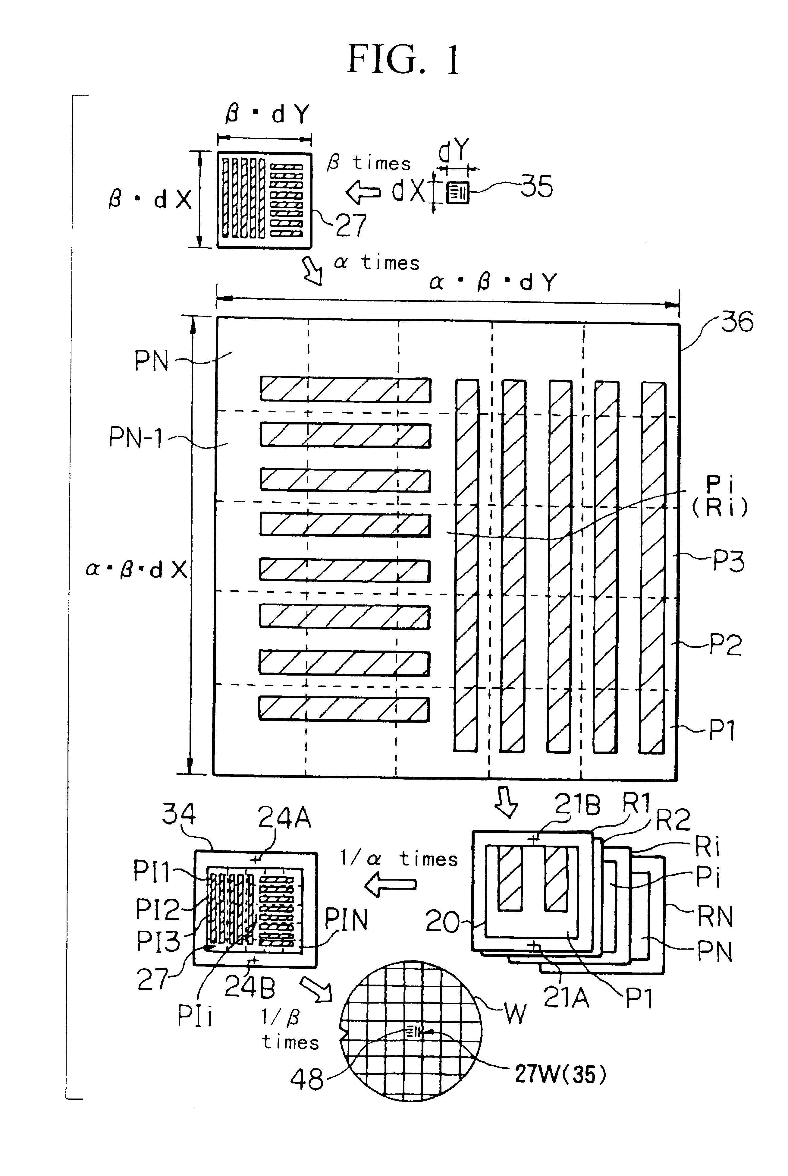
FIG. 1 is a diagram illustrating production steps for a photomask according to the first embodiment of this invention. In FIG. 1, a photomask to be produced is a working reticle 34 which is used at the time of actually manufacturing a semiconductor device. This working reticle 34 has an original pattern 27 for transfer formed of chromium (Cr), molybdenum silicide (MoSi.sub.2 or the like) or another mask material on one surface of a transmission substrate of quartz glass or the like. Two alignment marks 24A and 24B are formed in such a way as to sandwich the original pattern 27.

Further, the working reticle 34 is used in reduction projection of 1 / .beta. (.beta. is an integer, a half integer or the like greater than 1, and is 4, 5 or 6 or the like as one example) via the projection optical system of an optical projection exposure apparatus. That is, in FIG. 1, after a reduced image ...

second embodiment

A second embodiment of this invention will now be described with reference to the accompanying drawings.

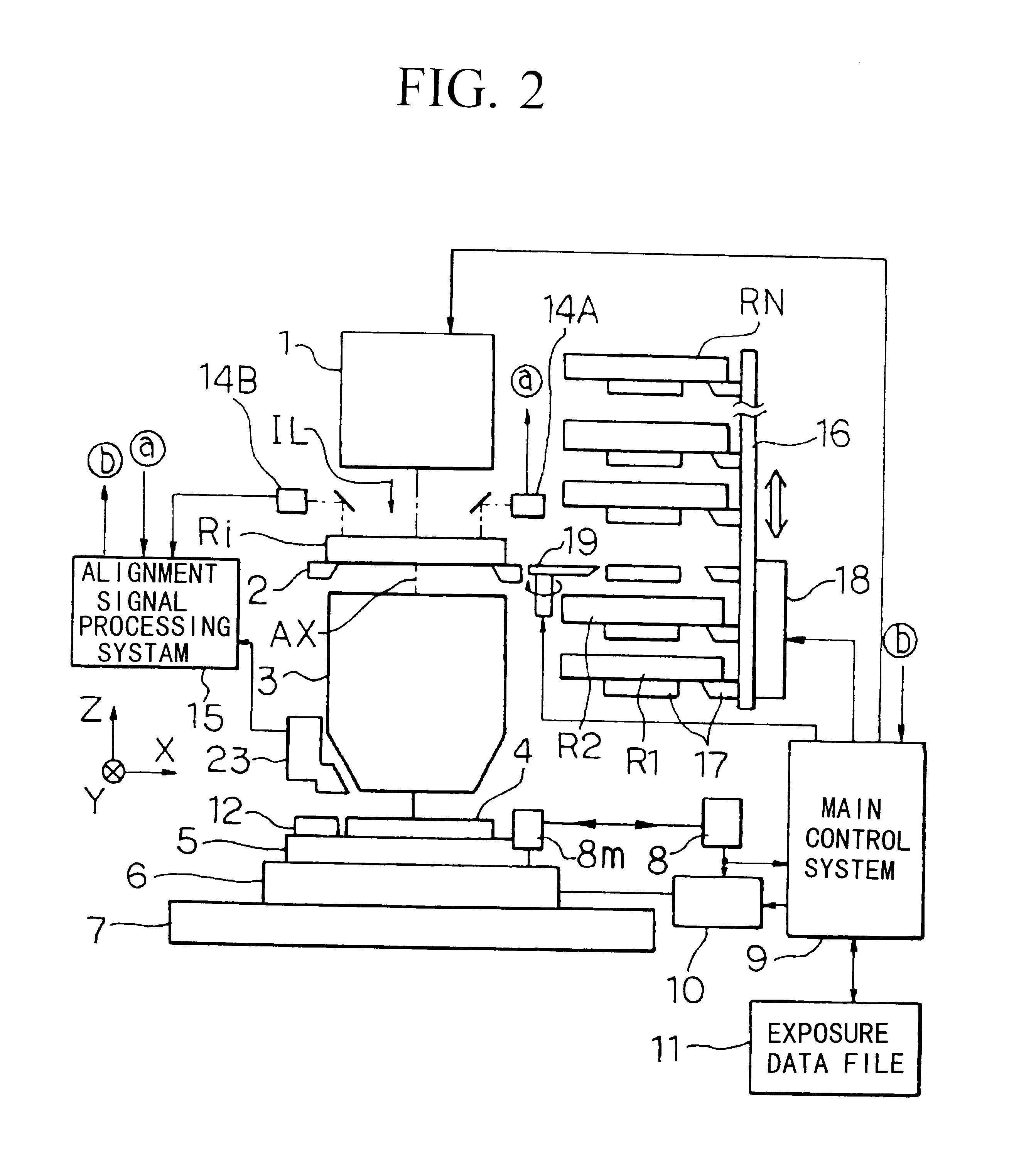
FIG. 7 is a diagram illustrating production steps for a photomask according to the second embodiment of this invention. In FIG. 7, as in FIG. 1, a photomask to be produced is the working reticle 34 that is used at the time of actually manufacturing a semiconductor device. This second embodiment differs from the first embodiment in that M sets (M being an integer greater than 2) of master reticles as parent masks are prepared and those plural sets of master reticles Ri, Qi . . . are used to produce the working reticle 34.

In FIG. 7, as in FIG. 1, first, the circuit pattern 35 is magnified by .beta. to form the original pattern 27 that has a rectangular area whose perpendicular sides have widths of .beta..multidot.dX and .beta..multidot.dY, on image data and then the original pattern 27 is magnified by .alpha. to form the parent pattern 36 that has a rectangular area whose perpendicu...

third embodiment

A third embodiment of this invention will now be described with reference to the accompanying drawings.

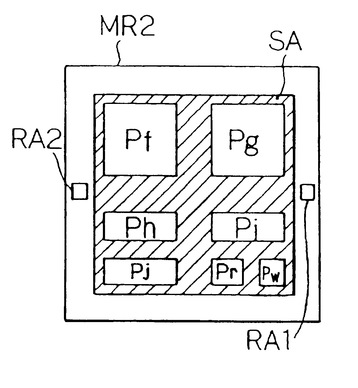
FIG. 13 is an explanatory diagram of a method of producing a photomask according to the third embodiment of this invention. As shown in FIG. 1C and FIG. 1D, photomasks to be produced in this example are working reticles WR, WR1 that are used at the time of actually manufacturing a semiconductor device. On those working reticles WR and WR1, patterns Pr equivalent to two alignment marks are so formed as to sandwich the original pattern, and a pattern Pw which becomes a wafer mark after being transferred onto the wafer is formed in the original pattern.

Further, the working reticles WR, WR1 of this example are used in reduction projection of 1 / .beta. via the projection optical system of an optical projection exposure apparatus as per the first and second embodiments.

The working reticle WR in this example is produced by forming a thin film of a mask material on a predetermined substrate...


PUM

PropertyMeasurementUnit
timeaaaaaaaaaa
wavelengthaaaaaaaaaa

Abstract

A photomask producing method according to the present invention segments a parent pattern which is an alpha-magnification of an original pattern which is a beta-magnification of a circuit pattern into alpha lengthwise and breadthwise, thereby forming parent patterns on data. The parent patterns are written on a substrate at equal magnification by using an electron beam lithography system, thereby producing master reticles. Reduced images of the parent patterns of the master reticles are transferred on a substrate while performing screen linking, thereby producing working reticle. This photomask producing method can form an original pattern with a high precision and in a short period of time.

Description

The present invention relates to a method and apparatus for producing a photomask which is used as an original pattern at the time of fabricating micro devices, such as semiconductor integrated circuits, image pickup devices (CCDs or the like), liquid crystal display devices or thin-film magnetic heads, by using lithographic technology. This invention also relates to a method of manufacturing a device which uses such a photomask producing method.At the time of manufacturing devices, such as semiconductor integrated circuits, a transfer system is employed which uses a photomask on which an original pattern that is a to-be-formed circuit pattern enlarged by, for example, about 4 to 5 times, and performs reduction projection of the original pattern of this photomask on a substrate to be exposed, such as a wafer or a glass plate, via a reduction projection optical system. An exposure system is used at the time of transferring the pattern of such a photomask and a photomask which is used...

Claims


Application Information

Patent Timeline
Patent Type & Authority Patents(United States)
IPC IPC(8): G03F7/20G03F1/14G03F1/00G03F1/78
CPCG03F1/14G03F1/78G03F7/70333G03F7/70475G03F7/2063H01J2237/31764H01L21/027
Inventor MAGOME, NOBUTAKASHIRAISHI, NAOMASA
Owner NIKON CORP
Why Eureka
Try Eureka