Wafer heating apparatus

a heating apparatus and a technology of a wafer, applied in the direction of ohmic-resistance heating, hot plate heating arrangements, coatings, etc., can solve the problems of long response time to the altered set temperature, insufficient moderated temperature distribution of the heating element, and long time-consuming to achieve the effect of heating and cooling to a set temperatur

Inactive Publication Date: 2004-06-22
KYOCERA CORP
View PDF5 Cites 418 Cited by
  • Summary
  • Abstract
  • Description
  • Claims
  • Application Information

AI Technical Summary

Problems solved by technology

However, the heat homogenizing plate 22 made of aluminum has a problem that it takes a long time to carry out heating and cooling to a set temperature and also it takes long to response to the altered set temperature due to a high thermal capacity.
However, in such a wafer heating apparatus described above, if the thickness of the heat homogenizing plate is made thin, the temperature distribution generated by the heating element is not sufficiently moderated and the temperature of the wafer W takes a long time to become even.
However, the thermoviewer has an temperature measurement error depending on the uneven hue of the surface of an object to be measured and the ambient environments and therefore is impossible to carry out measurement as precisely as required temperature precision.
When the heater disclosed in the foregoing Japanese Patent Application Laid-Open No. 6852 (2001) is subjected to measurement while such a temperature-measuring wafer is mounted on the apparatus, it is found difficult to satisfy the temperature dispersion within 0.5.degree. C.
Further, it is also found there exist points showing peculiar temperature values in the bent parts and gaps among patterns of the heating element formed for moderating the printing unevenness.
In the case of employing a conventional apparatus, even if heating is possible in a stable and saturated temperature state with even temperature distribution, when a wafer W cooled to a room temperature is mounted on a mounting face of the heating apparatus controlled to be at a prescribed temperature and heated, only the portions where the heat generation capacity is increased for even heating are sometimes heated quickly as compared with other portions to result in uneven temperature distribution during the transition time for heating.
Further, only the portions where the heat generation capacity is increased cause resistance alteration quickly and cause a problem that the temperature evenness is deteriorated within a short time.
Moreover, it is possible to improve the temperature evenness along with increase of the heat capacity in a heat homogenizing plate by increasing the thickness of the heat homogenizing plate, however that results in decrease of the thermal response and insensitivity of the temperature detection of thermocouples and accordingly, leads to an adverse result in temperature dispersion during the transition time for heating.
Such inconformity of the heat transmission manners results in occurrence of temperature difference-in-plane of the wafer and local change of the quality of a coating and uneven reaction of a resist film.
If P is smaller than 0.3 mm, the thickness in micro-order can not be stabilized in the case patterned resistor strips are formed by screen printing or the like to result in decrease of the reliability as the heating element and therefore, it is not preferable.
On the other hand, if the width G of the gap exceeds the above-described inequality, the gap becomes to wide and some portion of the heat homogenizing plate cannot sufficiently be heated to result in a wide temperature dispersion in the heat homogenizing plate.
On the other hand, in the case of the heat homogenizing plate with a thickness exceeding 8 mm, the plate takes a long time to respond to the temperature setting alteration and cooling, resulting in treatment efficiency decrease.
On the other hand, if the distance exceeds 0.5 mm, the heat transfer to a newly replaced wafer is decreased to deteriorate the temperature response and therefore it undesirably takes a long time to increase the temperature to a prescribed temperature.
On the contrary, in the case of exceeding 1.30 times, the heating element 5 does not improve the evenly heating property and in addition to that, the cost of the heat homogenizing plate is increased, the power consumption becomes high, and the cost of the apparatus itself is increased, and it is not preferably.
If the resistance temperature coefficient is too high, the resistance value at an ordinary temperature becomes low and the electric power supply at the time of starting power application is increased and a temperature control circuit for controlling the initial power becomes costly to increase the apparatus cost.
Next, in the case resin is used for the insulating layer 4, if the thickness is thinner than 30 .mu.m, the withstand voltage is less than 1.5 kV and the insulation property cannot be maintained, and when the heating element 5 is trimmed by laser radiation, the lower layer, the insulating layer 4, is damaged to result in deterioration of the insulating function.

Method used


Image

  • Wafer heating apparatus
  • Wafer heating apparatus
  • Wafer heating apparatus

Examples


embodiment 1

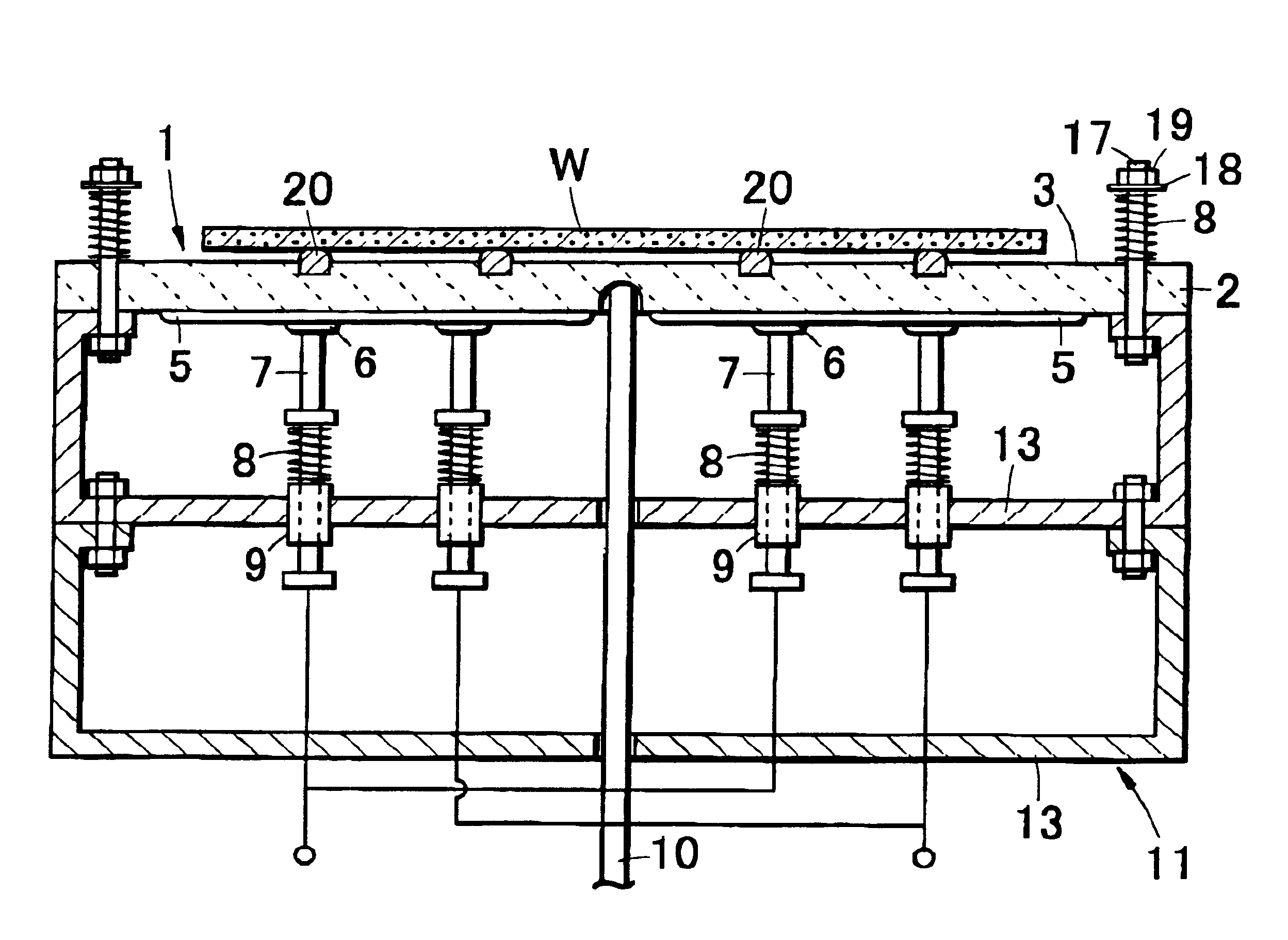
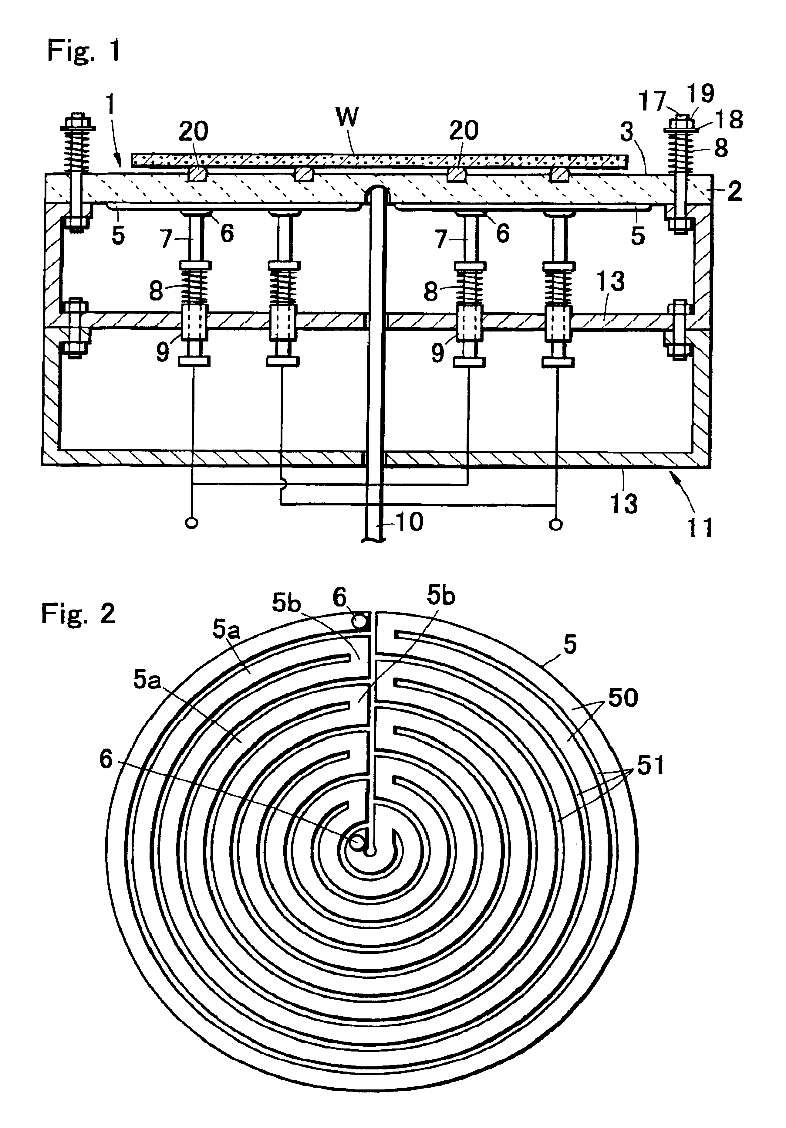
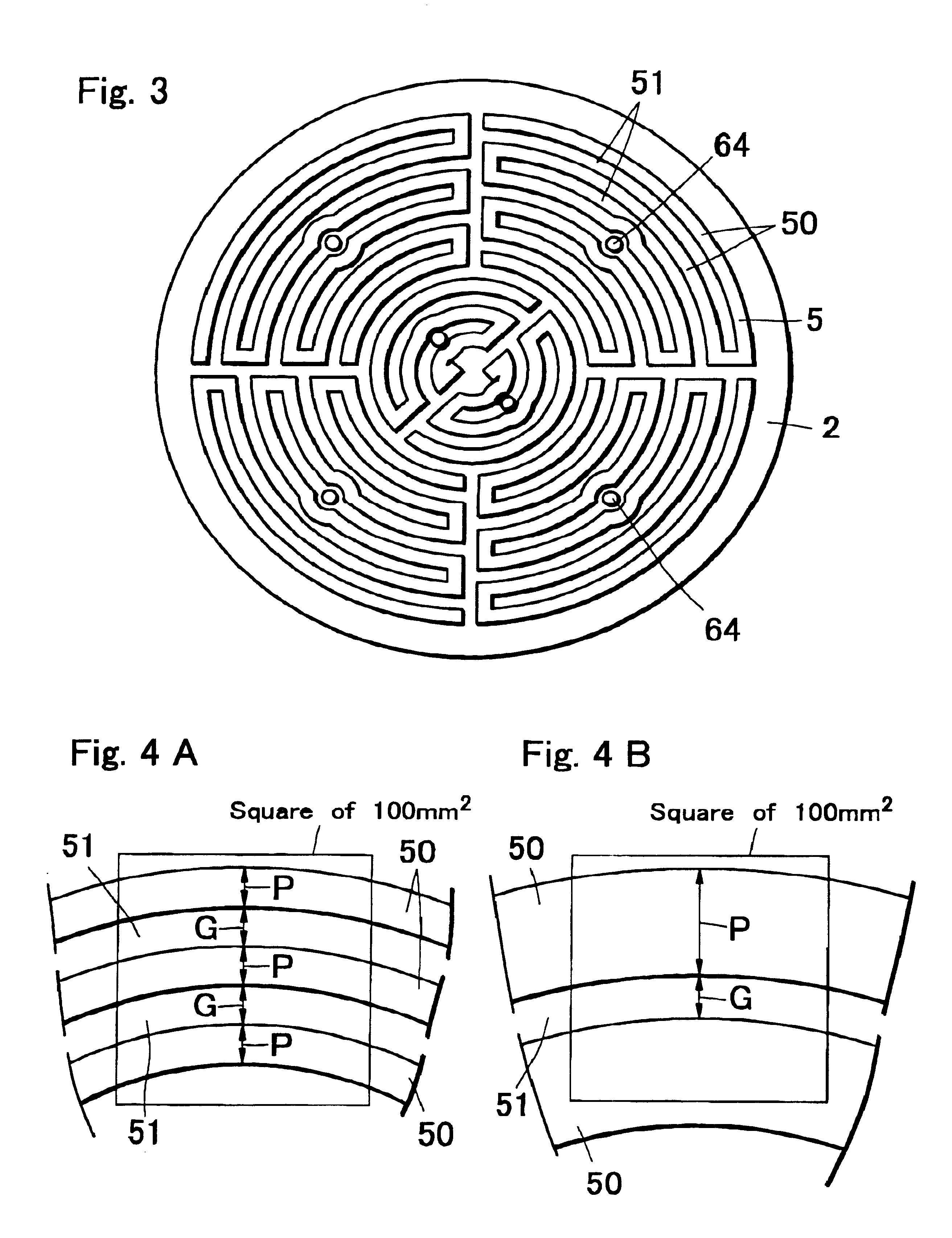
A plurality of heat homogenizing plates 2 with a disk-like shape of 3 mm thickness and 340 mm outer diameter were produced by grinding and polishing a silicon carbide sintered-based body with a thermal conductivity of 100 W / m / K and in order to form an insulating layer 4 on one main face of each heat homogenizing plate 2, a glass paste produced by kneading a glass powder with ethyl cellulose as binder and terpineol as an organic solvent was applied by a screen printing method and heated to 150.degree. C. for drying the organic solvent. After that, degreasing treatment was carried out at 550.degree. C. for 30 minutes and further baking was carried out at a temperature from 700 to 900.degree. C. to form the insulating layer 4 of glass with a thickness of 200 .mu.m. Then, in order to form a heating element 5 on the insulating layer 4, a paste produced by mixing 20% by weight of a Au powder and 10% by weight of a Pt powder as conductive materials, 70% by weight of glass, and prescribed a...

embodiment 2

A plurality of heat homogenizing plate s 2 with a disk-like shape of a thickness of 3 mm and an outer diameter of 300 mm, 315 mm, 340 mm, and 375 mm were produced by grinding and polishing a silicon carbide sintered-based body with a thermal conductivity of 100 W / m / K and in order to form an insulating layer 4 on one main face of each heat homogenizing plate 2, a glass paste produced by kneading a glass powder with ethyl cellulose as binder and terpineol as an organic solvent was applied by a screen printing method and heated to 150.degree. C. for drying the organic solvent. After that, degreasing treatment was carried out at 550.degree. C. for 30 minutes and further baking was carried out at a temperature from 700 to 900.degree. C. to form the insulating layer 4 of glass with a thickness of 200 .mu.m. Then, in order to form a heating element 5 on the insulating layer 4, a paste produced by mixing 20% by weight of a Au powder and 10% by weight of a Pt powder as conductive materials, ...

embodiment 3

An alumina sintered body of a thermal conductivity of 30 W / m / K, an aluminum nitride sintered body of a thermal conductivity of 50 W / m / K, and silicon carbide-based sintered bodies of a thermal conductivity of 80 W / m / K and 150 W / m / K, respectively, were employed. These sintered bodies were ground and polished to produce a large number of heat homogenizing plate s 2 with a disk-like shape of 1 mm thickness and 340 mm outer diameter.

In order to form an insulating layer 4 on one main face of each heat homogenizing plate 2, a glass paste produced by kneading a glass powder with ethyl cellulose as binder and terpineol as an organic solvent was applied by a screen printing method and heated to 150.degree. C. for drying the organic solvent. After that, degreasing treatment was carried out at 550.degree. C. for 30 minutes and further baking was carried out at a temperature from 700 to 900.degree. C. to form the insulating layer 4 of glass with a thickness of 200 .mu.m. Then, in order to form a...


PUM

PropertyMeasurementUnit
thicknessaaaaaaaaaa
distanceaaaaaaaaaa
outer diameteraaaaaaaaaa

Abstract

In a ceramic heater having a plate-like body made of a ceramic, heating element in one main face of the plate like body, and an electric supply portion to be electrically connected with the heating element, it has been a problem that the temperature is uneven if bent portions are formed in heat generating patterns. The ceramic heater simultaneously satisfying the following: 0.15<=S<=0.85, 0.3<=P<=6.71XS<2>+1.52, and 0.3<=G<=6.71x(1-S)<2>+1.55, in which the reference character S1 denotes the surface area of the heating element in optional 10 mm square region of the effective heat generation area having the heating element therein; the surface ratio S denotes S=S1 / 100 mm<2>, the reference character P denotes the width of the heating element: and the reference character G denotes the gap between the heating element.

Description

1. Field of the InventionThe present invention relates to a wafer heating apparatus to be employed for heating mainly a wafer and a ceramic heater to be employed for the apparatus and for example to a wafer heating apparatus suitable for forming a semiconductor thin film on a semi conductor wafer, a liquid crystal substrate, a circuit board or the like and for forming a resist film by drying and baking a resist liquid applied to the water.2. Prior ArtIn semiconductor thin film formation treatment, etching treatment, resist film baking treatment and the like in semiconductor device fabrication process, a wafer heating apparatus is employed for heating a semiconductor wafer.Conventionally, the wafer heating apparatus has been made to be a batch type apparatus for carrying out film formation treatment of a plurality of wafers. Along with the recent tendency to enlarge a wafer size from 8 to 12 inches, a sheet-fed manner for heating wafers one by one has been employed to increase the tr...

Claims


Application Information

Patent Timeline
Patent Type & Authority Patents(United States)
IPC IPC(8): H01L21/00H05B3/14H05B3/26H05B3/22H01L21/324
CPCH01L21/67103H05B3/143H05B3/265H01L21/324
Inventor FURE, HIROSHINAGASAKI, KOICHIUCHIYAMA, KYOJI
Owner KYOCERA CORP
Why Eureka
Try Eureka