Method and apparatus for optimizing exposure time in image acquisitions

a technology for image acquisition and exposure time, applied in the field of image sensors, can solve the problems of low yield of integrated circuit chips containing ccd image sensors, high cost, and inability to address the problem of ccds, and achieve the effect of optimizing the exposure of an image acquisition system

Inactive Publication Date: 2004-07-20
PIXIM
View PDF13 Cites 114 Cited by
  • Summary
  • Abstract
  • Description
  • Claims
  • Application Information

AI Technical Summary

Problems solved by technology

Integrated circuit chips containing a CCD image sensor have a relatively low yield and are expensive due to the specialized processing involved.
The CCDs also consume a relatively large amount of power.
However, none of the present technologies have addressed the issue of photodetectors reaching saturation in certain areas of the image sensor array before the rest of the photodetectors in the image sensor array do.
This causes problems with over or under exposure of the image sensor array.

Method used


Image

  • Method and apparatus for optimizing exposure time in image acquisitions
  • Method and apparatus for optimizing exposure time in image acquisitions
  • Method and apparatus for optimizing exposure time in image acquisitions

Examples


Embodiment Construction

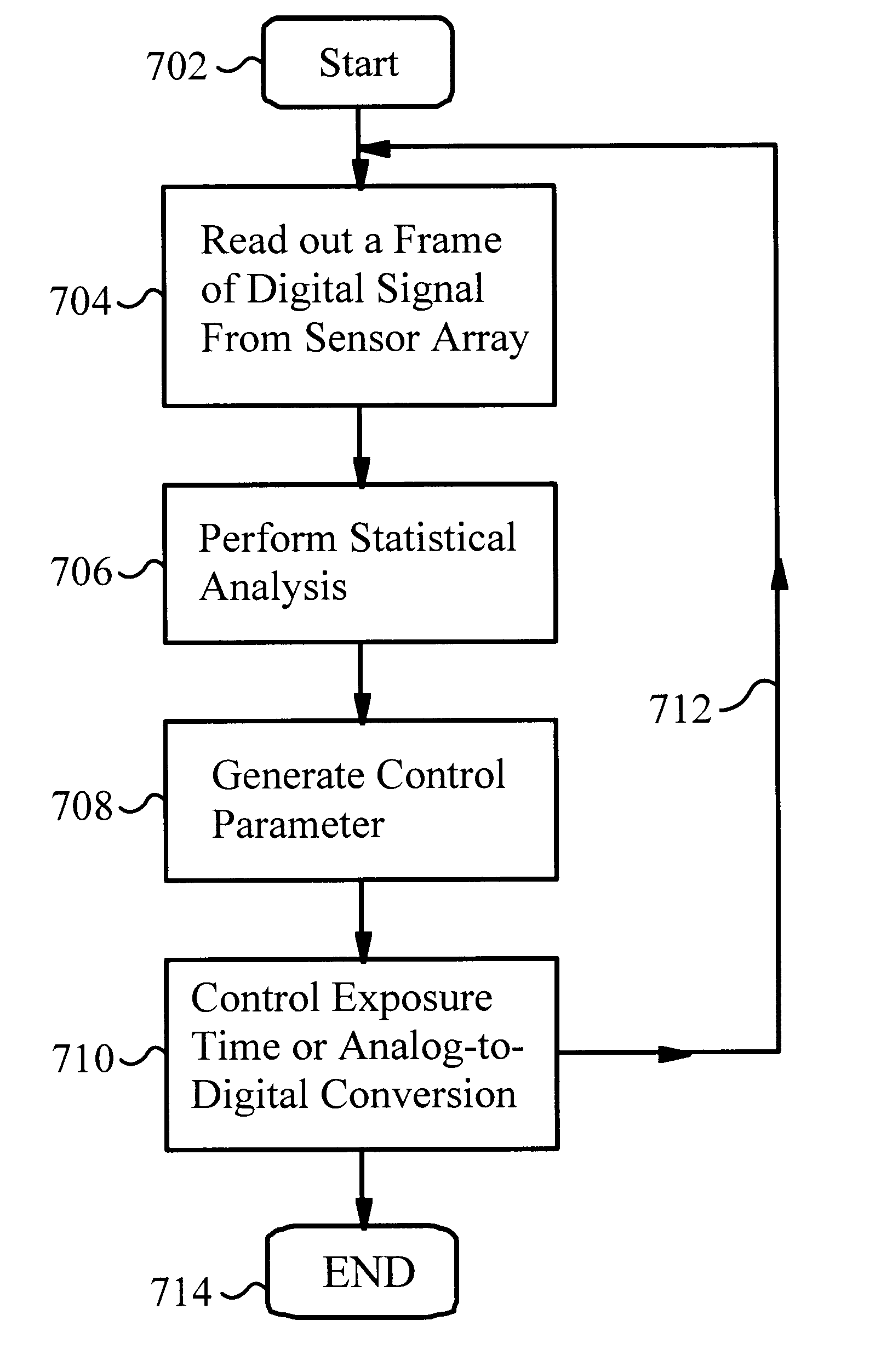
Although the following detailed description contains many specifics for the purposes of illustration, anyone of ordinary skill in the art will appreciate that many variations and alterations to the following details are within the scope of the invention. Accordingly, the following preferred embodiment of the invention is set forth without any loss of generality to, and without imposing limitations upon, the claimed invention.

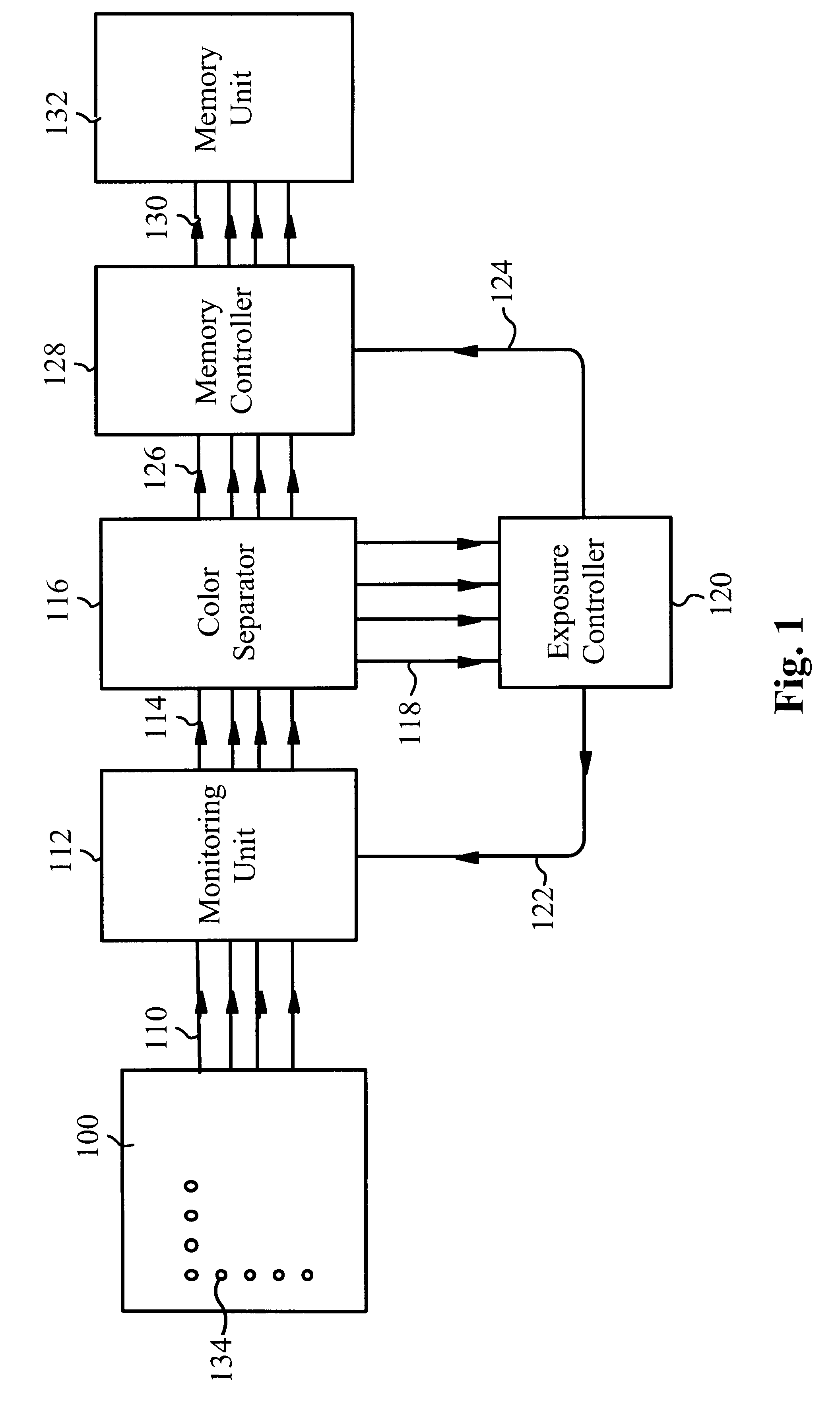
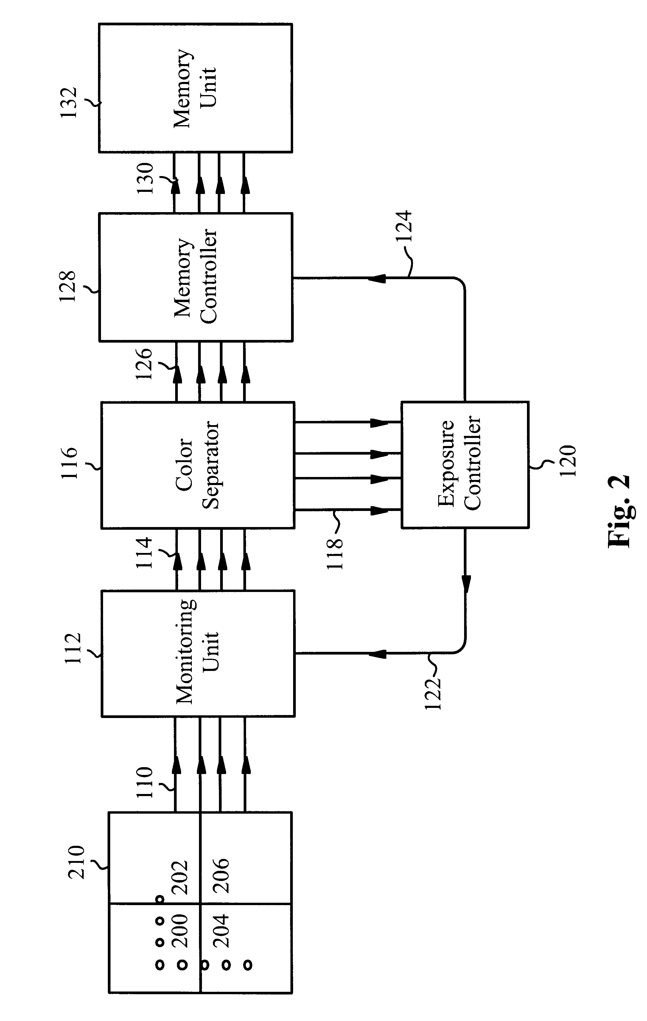
FIG. 1 shows an embodiment of the present invention. An image sensor array 100 comprises thousands of pixels 134, which can be arranged in a 2-dimensional array of rows and columns.

Each pixel comprises a photodetector and an analog-to-digital converter (ADC). The photodetectors can be any device with a conductivity that is proportional to the light intensity that is impinging upon it. Examples of such devices are charge coupled device (CCD) and CMOS phototransistors. The analog current that is flowing through a phototransistor or photogate is proportional to the...


PUM


Abstract

A method of optimizing the exposure times of regions of pixels of an image sensor array during exposure is accomplished by utilizing time interval sampling of an image sensor array comprising of pixels configured to generate digital image signals. Luminance values are extracted from each digital image signal and analyzed to determine if a pixel has reached the optimal exposure. If a pixel has reached the optimal exposure, subsequent digital image signals from this pixel will not be recorded. This preserves the recording of the optimal digital image signal generated by the pixel at the time when the pixel reached its optimal exposure. This process of selectively terminating the recording of digital image signals based on optimal exposures of the pixels can be performed on individual pixels or can be performed on a region of pixels.

Description

1. Field of the InventionThe present invention relates to image sensors for converting an optical image into electrical signals and particularly to a method and apparatus for optimizing exposure time in image acquisitions.2. Description of the Related ArtAn image sensor is used to convert an optical image focused on the sensor into electrical signals. The image sensor typically includes an array of photodetectors, where each photodetector produces a signal corresponding to the intensity of light impinging upon that photodetector when an image is focused on the array. These signals may then be used, for example, to display a corresponding image on a monitor or otherwise used to provide information about the optical image.One very common type of image sensor is a charge coupled device (CCD). Integrated circuit chips containing a CCD image sensor have a relatively low yield and are expensive due to the specialized processing involved. The CCDs also consume a relatively large amount of ...

Claims


Application Information

Patent Timeline
Patent Type & Authority Patents(United States)
IPC IPC(8): H04N5/235G03B7/093G03B7/28G01J1/44
CPCH04N5/2351H04N5/2353H04N23/71H04N23/73H04N23/70H04N25/62
Inventor DENG, ZHONGHANYANG, DAVID XIAO DONGPENG, XIEWEDEMI, ODUTOLA OLUSEYEMOTTA, RICARDO JANSSONWEI, YI-HEN
Owner PIXIM
Why Eureka
Try Eureka