Method of attaching an integrated circuit to a chip mounting receptacle in a PCB with a bolster plate

a technology of integrated circuits and mounting receptacles, which is applied in the field of electrical equipment manufacture, can solve the problems of affecting the desired electrical contact, and affecting the electrical contact of the integrated circuit chip

Inactive Publication Date: 2004-09-14
HEWLETT-PACKARD ENTERPRISE DEV LP
View PDF1 Cites 23 Cited by
  • Summary
  • Abstract
  • Description
  • Claims
  • Application Information

AI Technical Summary

Problems solved by technology

The printed circuit boards, alone, lack sufficient rigidity to support the compressive loads during attachment.
Resultant bending of the printed circuit board is capable of damaging wiring or other materials within the integrated circuit chip.
Additionally, the bending moment is capable of disrupting the desired electrical contact.
It has been discovered that the use of a bolster plate according to traditional practices does not sufficiently eliminate the bending moment in the printed circuit boards in light of these new demands.
Even this small amount of bending is sufficient damage the assembly or to cause failure in the electrical contact.
The increased thickness creates other difficulties in the context of fitting additional components on the printed circuit board and in assembling adjacent components in the intended use environment.
Attempts have been made to pre-bow or pre-stress the bolster plate to accommodate the stress during the attachment of microprocessors, but the resulting bending moment from pre-stressing the bolster plate was not repeatable.
There remains a problem in preventing bolster plate bending due to the insertion of newer microprocessors and ASICS devices.

Method used


Image

  • Method of attaching an integrated circuit to a chip mounting receptacle in a PCB with a bolster plate
  • Method of attaching an integrated circuit to a chip mounting receptacle in a PCB with a bolster plate
  • Method of attaching an integrated circuit to a chip mounting receptacle in a PCB with a bolster plate

Examples


Embodiment Construction

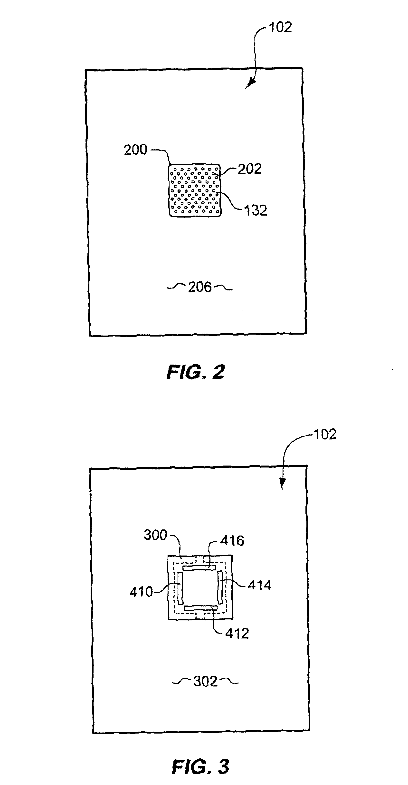
There will now be shown by way of example and not by limitation, a bolster plate in use for supporting a printed circuit board during attachment of an integrated circuit chip to the printed circuit board. The bolster plate comprises a support rail presenting a contact face for use in contacting the printed circuit board. The rail demarcates a central well that contains a support surface configured to support a selected portion of the printed circuit board underneath the integrated circuit chip during attachment of the integrated circuit chip to the printed circuit board.

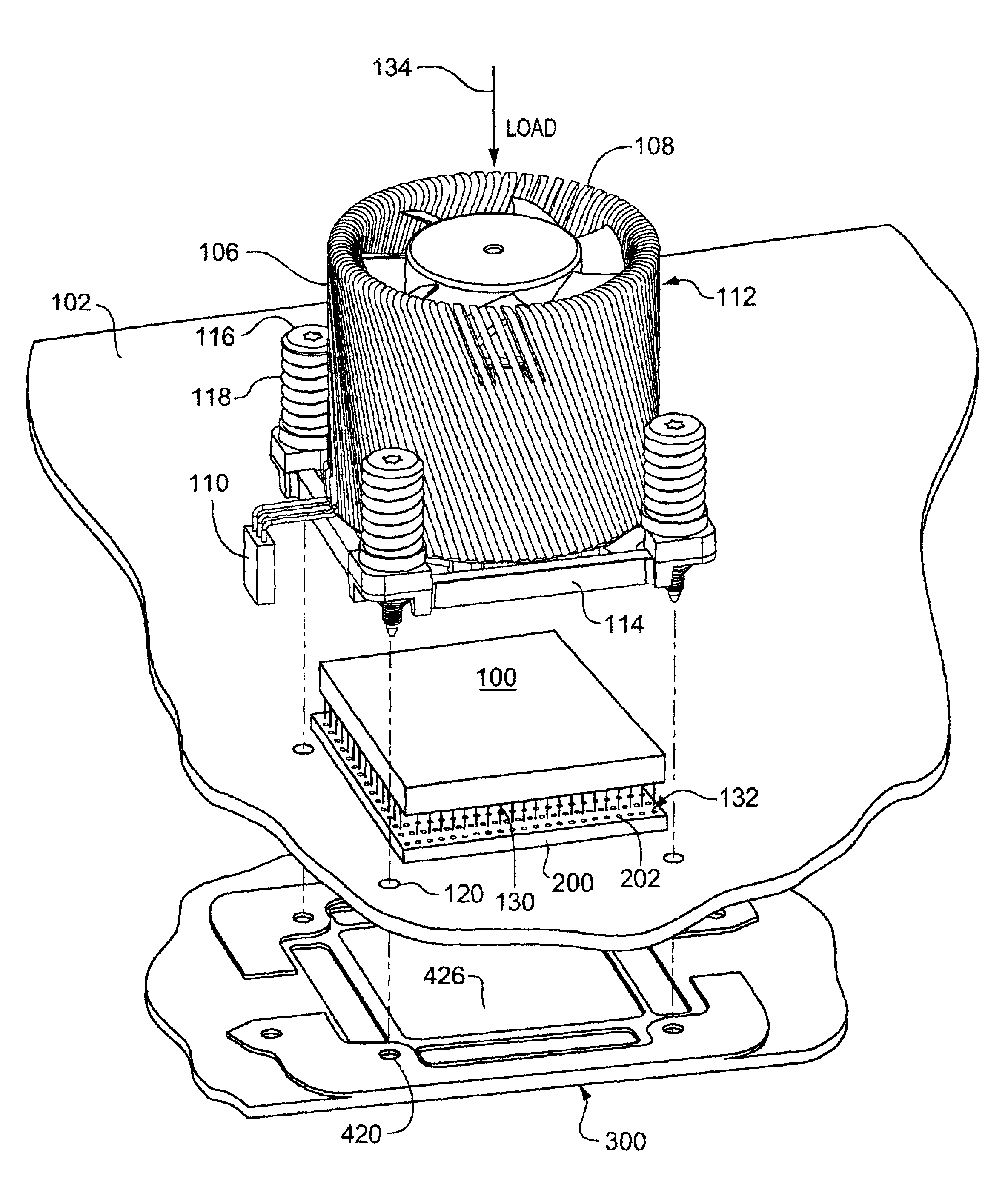
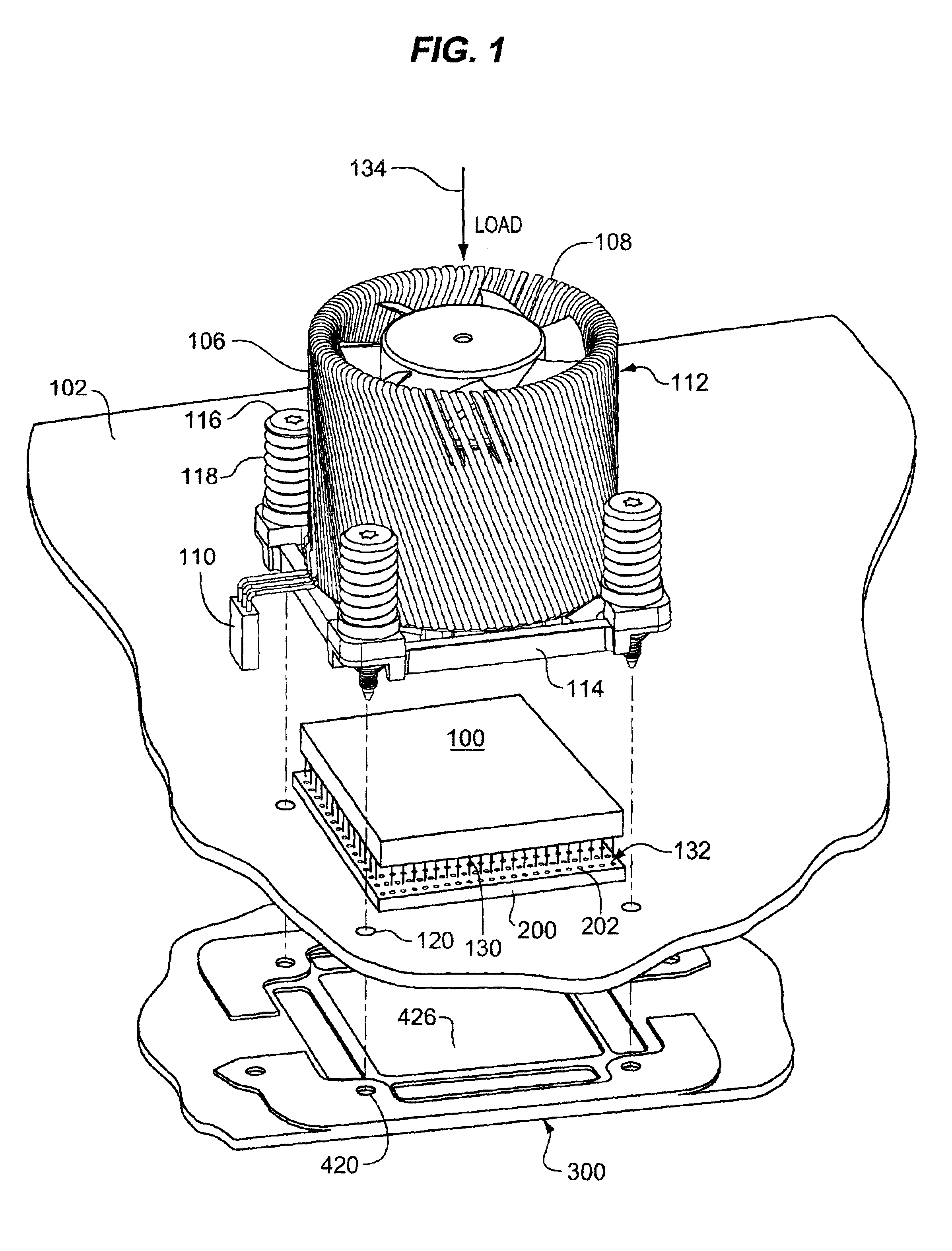
FIG. 1 is an assembly view showing an integrated circuit chip 100, e.g., a microprocessor, that is being attached to a printed circuit board 102 by insertion into a chip socket 200. A heat sink assembly 106 comprises a central electric fan 108 with a corresponding power coupling 110, and well as heat-conductive fins 112. A square base plate 114 at each corner contains a shoulder screw, such as screw 116, that is circ...


PUM

PropertyMeasurementUnit
forceaaaaaaaaaa
distanceaaaaaaaaaa
areaaaaaaaaaaa

Abstract

A bolster plate is attached to a printed circuit board and acts as a stiffener that reduces bending in the overall assembly during the attachment of an integrated circuit chip to the printed circuit board under a heavy applied load. The bolster plate is provided with a shim that compensates for bending of the bolster plate under load, thereby preventing damage to the integrated circuit chip. The dimensions of the shim may be selected according to computer model results representing bow deformation in the bolster plate without the shim.

Description

1. Field of the InventionThe invention pertains to the field of electrical equipment manufacture and, particularly, the electrical attachment of integrated circuit chips, such as microprocessors and application-specific integrated circuits (ASICS), to printed circuit boards. More specifically, the method of attachment uses a bolster plate to reinforce the printed circuit board during the attachment process.2. Discussion of the Related ArtA variety of methods have been devised for the attachment of integrated circuit chips, such as microprocessors and ASCIS, to printed circuit boards in a manner that assures consistency in establishing good electrical contact. Many of these methods involve the use of high compressive loads, which are applied to the processors. The integrated circuit chips typically have a plurality of pins that mate with a corresponding female conductive receptacle in the printed circuit board. The printed circuit boards, alone, lack sufficient rigidity to support th...

Claims


Application Information

Patent Timeline
Patent Type & Authority Patents(United States)
IPC IPC(8): H05K7/10H05K13/04
CPCH05K7/1084Y10T29/53178Y10T29/49004Y10T29/53265Y10T29/53174Y10T29/53983Y10T29/49126Y10T29/4913Y10T29/53961Y10T29/53978Y10T29/53974
Inventor WHITE, JOSEPH M
Owner HEWLETT-PACKARD ENTERPRISE DEV LP
Why Eureka
Try Eureka