Semiconductor device having a primary chip with bumps in joined registration with bumps of a plurality of secondary chips

a secondary chip and primary chip technology, applied in semiconductor devices, semiconductor/solid-state device details, electrical apparatus, etc., can solve the problems of reducing requiring a long time period for assembling, and a large probability of secondary chips being erroneously bonded or mounted, etc., to achieve the effect of improving the production efficiency of secondary chips

Inactive Publication Date: 2005-01-04
ACHLYS TECH INC
View PDF19 Cites 3 Cited by
  • Summary
  • Abstract
  • Description
  • Claims
  • Application Information

AI Technical Summary

Benefits of technology

A first object of the present invention is to provide, in a semiconductor device having a structure in which a plurality of semiconductor chips are joined to a surface of a solid, a semiconductor device having a structure in which the production efficiency thereof can be improved.

Problems solved by technology

Therefore, a long time period is required for assembling.
Since there are a plurality of secondary chips, the probability that the secondary chips are erroneously bonded or mounted (an erroneous mounting rate) is considerably high.

Method used


Image

  • Semiconductor device having a primary chip with bumps in joined registration with bumps of a plurality of secondary chips
  • Semiconductor device having a primary chip with bumps in joined registration with bumps of a plurality of secondary chips

Examples


Embodiment Construction

In embodiments of the present invention described below, it is presupposed that Si is used as the type of semiconductor. However, another semiconductor such as GaAs or Ge may be used.

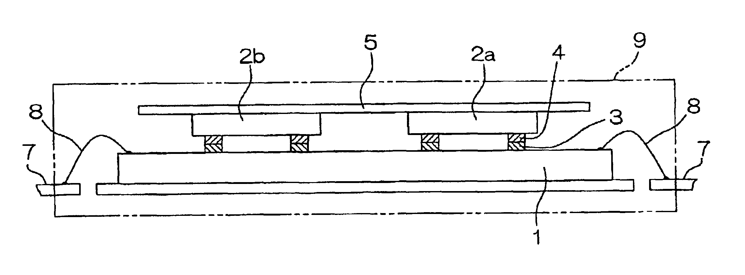
FIG. 1 is a side view showing a state where a plurality of secondary chips 2a and 2b are overlapped with a primary chip 1 by so-called face-down bonding. Bumps 3 are provided on a device formation surface of the primary chip 1, and bumps 4 are also provided in corresponding positions on device formation surfaces of the secondary chips 2a and 2b. The corresponding bumps 3 and 4 are joined to each other, thereby having assembled a semiconductor device having a so-called chip-on-chip structure.

The secondary chips 2a and 2b are in a state where they are mounted on one common frame 5. A material for the frame 5 is not particularly limited. Examples are a resin plate, a glass plate, a metal plate, a ceramic plate, and the like, which are transparent or opaque. Further, the thickness of the frame 5 is not part...


PUM


Abstract

A semiconductor device having a plurality of semiconductor chips respectively joined to predetermined positions on a surface of a solid, and a frame holding the plurality of semiconductor chips in a relative positional relationship corresponding to joint positions on the surface of the solid. The solid may be another semiconductor chip or a wiring board. The plurality of semiconductor chips may be bonded to a surface, opposite to the surface, of the solid, of the frame. The plurality of semiconductor chips may be respectively fitted in through holes formed in the frame.

Description

BACKGROUND OF THE INVENTION1. Field of the InventionThe present invention relates generally to a semiconductor device, and more particularly, to a semiconductor device having a structure in which a plurality of semiconductor chips are bonded to a surface of a solid (for example, a semiconductor chip or a wiring board) and a method of assembling the same.2. Description of Related ArtIn order to increase a substantial integration degree of a semiconductor device, a semiconductor device having a chip-on-chip structure in which semiconductor chips in two layers are overlapped with each other has been paid attention to.Specifically, a pad opening where internal wiring is partially exposed is provided on a device formation surface of each of semiconductor chips to be overlapped, for example. A projection electrode called a “bump” is provided in the pad opening. The semiconductor chips are overlapped with each other by so-called face-to-face bonding.For example, one of the semiconductor ch...

Claims


Application Information

Patent Timeline
Patent Type & Authority Patents(United States)
IPC IPC(8): H01L25/065H01L25/18H01L23/02H01L25/07
CPCH01L25/0655H01L2224/16225
Inventor HIKITA, JUNICHIYAMAMOTO, KOJI
Owner ACHLYS TECH INC
Why Eureka
Try Eureka