Method for applying a substrate

a substrate and substrate technology, applied in the direction of lamination ancillary operations, lamination apparatus, electrical apparatus, etc., can solve the problems of uneven rear side of the wafer, and inability to apply a substrate uniformly, so as to minimize the possibility of air bubble inclusion, optimize the reduction of the thickness of the wafer, and reduce the possibility of microcracks

Inactive Publication Date: 2005-01-11
SUSS MICROTEC LAB EQUIP
View PDF8 Cites 13 Cited by
  • Summary
  • Abstract
  • Description
  • Claims
  • Application Information

AI Technical Summary

Benefits of technology

One object of this invention is to provide a method and apparatus to connect the wafer to the protective layer without excessive process cost expenses and without any problems, with extensive exclusion of air bubbles.
According to a further embodiment of this invention, the wafer is exposed to almost constant pressure as it is laid onto the protective layer. This ensures a largely constant, uniform and only small depth of penetration of the wafer into the protective layer. This is achieved during the linear approach movement of the pre-shaped wafer towards the protective layer by constantly monitoring the spacing between the two bodies. As soon as the dome-shaped contact point reaches the protective layer, the speed and the spatial shape of the wafer are correspondingly altered so that the surface area of the dome-shaped wafer extends two-dimensionally over the protective layer, without causing significant locally varying depths of penetration.
The method makes it possible to provide the active side of the wafer with a protective layer and to minimize the possible inclusion of air bubbles. Thus in the following working step, the rear side of the wafer is not impaired by unevenness. With the method of this invention it is possible to optimize the reduction of the wafer thickness.
Furthermore through a favorable initial position of the surface, possible damage, such as microcracks, can be reduced.

Problems solved by technology

Unevenness impairs the rear side of the wafer which is to be processed.
It has become apparent, that despite expensive preparation of the wafer substrate, there is an inherent disadvantage in the system.
Through the introduction of a protective layer between the active side of the wafer and the assembly carrier, air pockets occur which cause unevenness on the rear side of the wafer.
These air pockets can scarcely be eliminated by increasing the compressive force or distributing the local pressure locations.
Repeating the pressing process several times also does not achieve the desired result.
Moreover, the danger of breaking the wafer is increased in an uncontrolled manner by such manipulations.

Method used


Image

  • Method for applying a substrate
  • Method for applying a substrate
  • Method for applying a substrate

Examples


Embodiment Construction

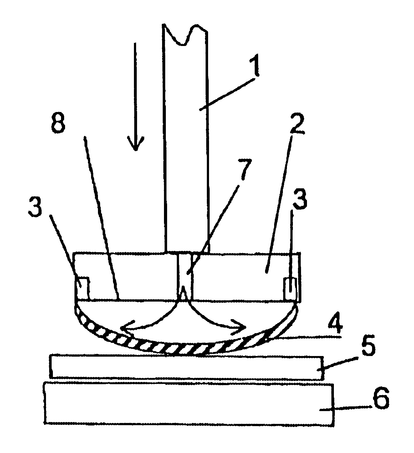
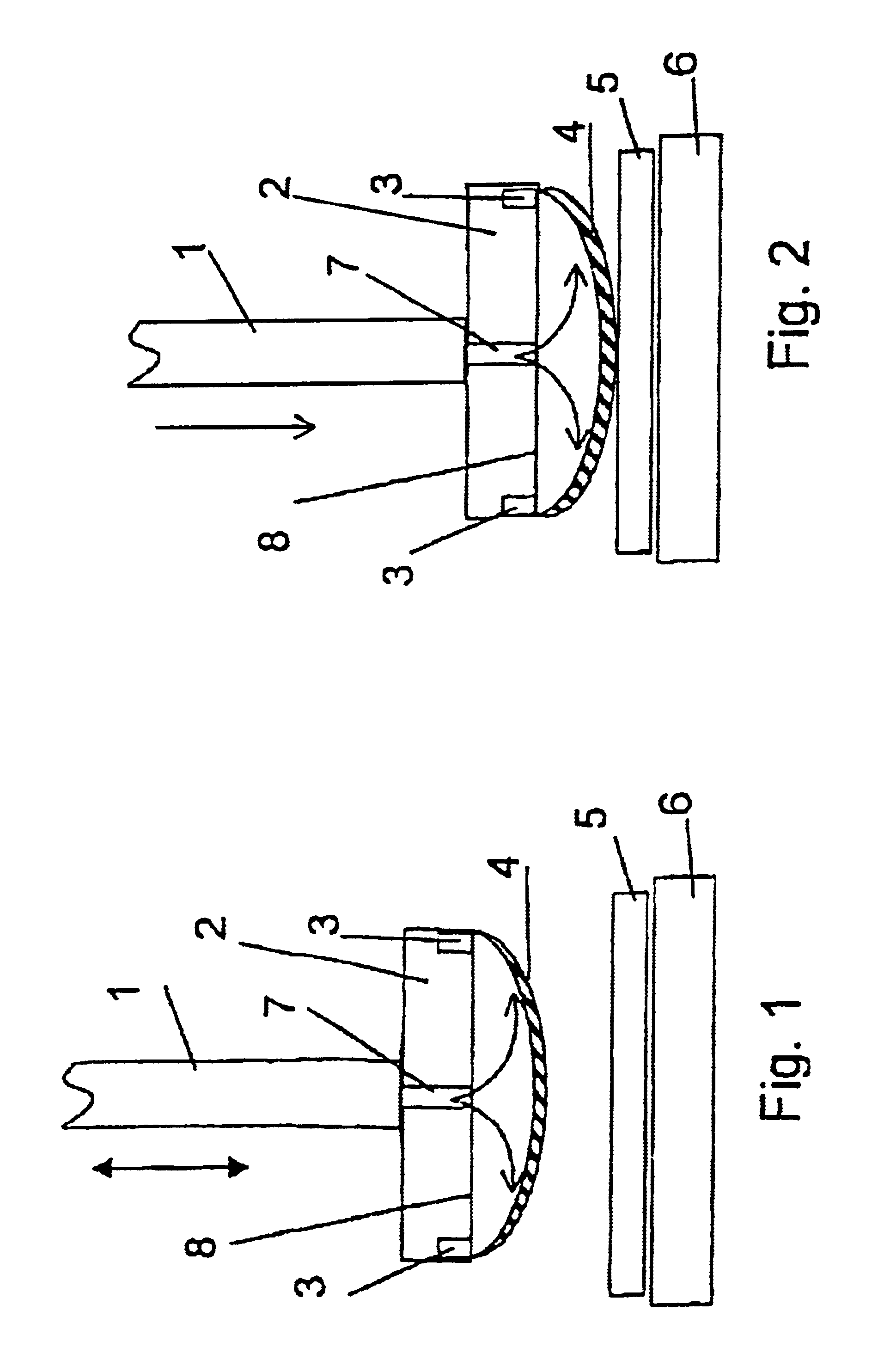
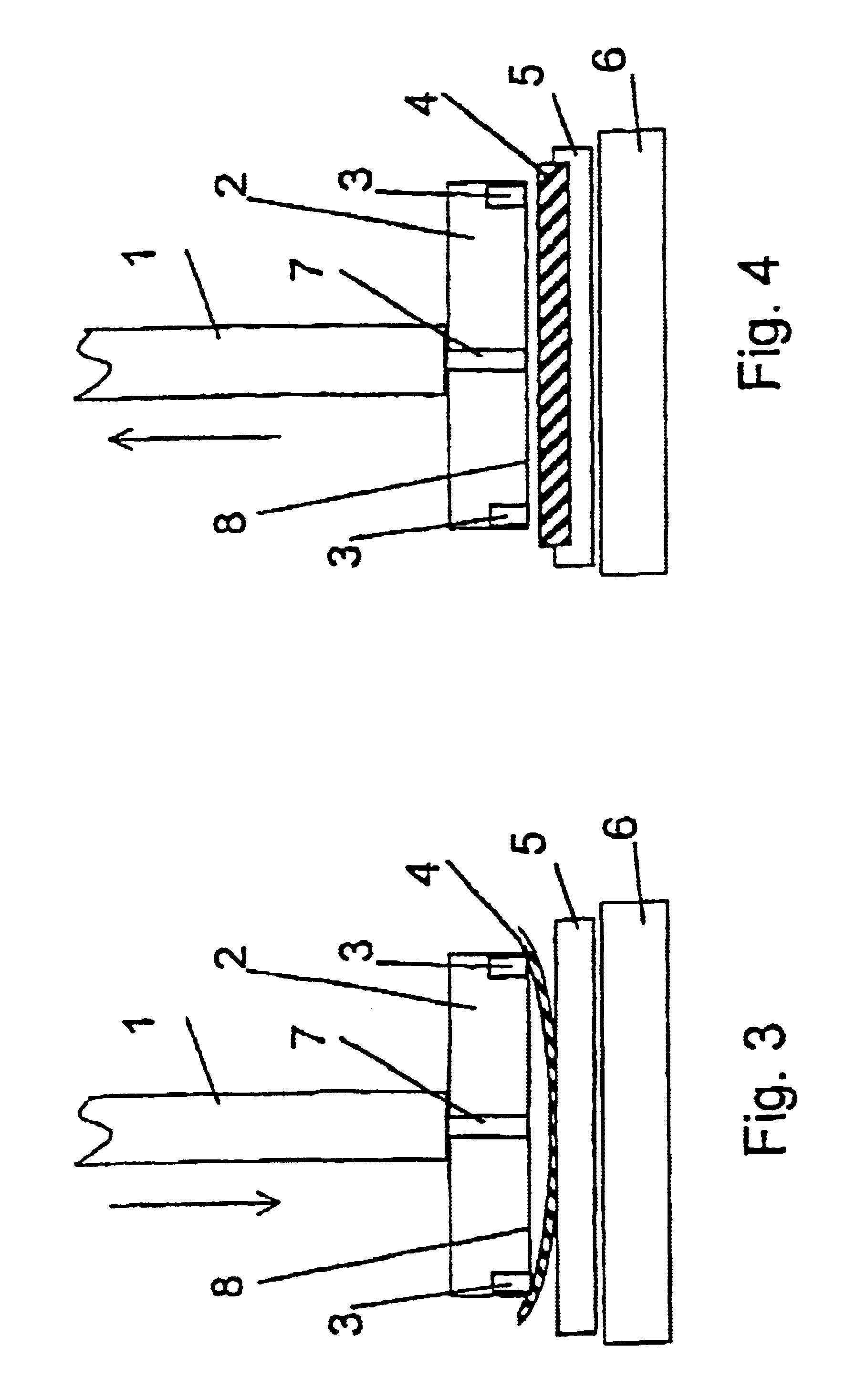
FIGS. 1 to 4 show four steps of a chronological progression of the method for applying the active side of the substrate or wafer 4 into the protective layer 5. The initial phase of the process is shown in FIG. 1. The feed arm 1 guides the carrying body 2 in a linear movement to the assembly carrier 6, to which the prepared protective layer 5, such as a wax, is applied. The carrying body 2 has a lower portion 8 which can have a shape, when viewed from above, of one of circular, oval and polygonal. The carrying body 2 has on its lower portion 8 one or a plurality of preferably central open ducts, each of which is supplied with excess pressure by a pressure medium, such as air or another fluid. Groove-shaped flow apertures 3, 7, through which the medium is extracted, are attached in an arc on the periphery of the lower portion 8. This negative pressure in the initial phase holds and fixes the wafer 4 at the edges of its rear side. As soon as sufficient retention force is achieved by su...


PUM

PropertyMeasurementUnit
thicknessaaaaaaaaaa
pressureaaaaaaaaaa
constant pressureaaaaaaaaaa

Abstract

A method for applying a thin-walled, flat substrate, such as a wafer, to an assembly carrier with a preferably level protective layer, for example a wax. With respect to the protective layer, the substrate is arranged at a spacing and is curved in a convex manner. The substrate is contacted with the protective layer. Finally, the substrate is laid over the entire protective layer from the contact point towards the edge of the substrate.

Description

BACKGROUND OF THE INVENTION1. Field of the InventionThis invention relates to a method for applying a substrate, such as a wafer to an assembly carrier, and to a device for accomplishing this method.2. Description of Related ArtIn the commercial production of semiconductor wafers, such as slices of silicon, GaAs and the like, a semiconductor wafer is subjected to different successive processes. An important step after applying various structures and layers on a front side, such as an active side or respectively the side on which the applied structures are located, is the attachment of a protective layer on the active side. This layer protects the upper side of the wafer and thus its sensitive surface during the subsequent treatment process, for example thinning the wafer by grinding or lapping. The thinning process takes place on the rear side of the wafer and significantly influences the residual thickness of the wafer.Because abrading occurs down to a thickness of approximately 50...

Claims


Application Information

Patent Timeline
Patent Type & Authority Patents(United States)
IPC IPC(8): H01L21/00H01L21/683H01L21/68H01L21/67H01L21/302
CPCB32B37/0007B32B38/1866H01L21/6838H01L21/6835H01L21/67132
Inventor MUFFLER, PIRMIN GERHARD
Owner SUSS MICROTEC LAB EQUIP
Why Eureka
Try Eureka