Method for manufacturing self-aligned BiCMOS

a technology of bipolar transistors and manufacturing methods, applied in the direction of basic electric elements, electrical apparatus, semiconductor devices, etc., can solve the problems of reducing the integration density, degrading the performance of the transistor, and more defects in the fabrication process

Active Publication Date: 2005-01-25
SAMSUNG ELECTRONICS CO LTD
View PDF6 Cites 41 Cited by
  • Summary
  • Abstract
  • Description
  • Claims
  • Application Information

AI Technical Summary

Benefits of technology

The present invention provides a method for manufacturing a self-aligned BiCMOS, by which a SiGe HBT can be formed without degradation due to misalignment.

Problems solved by technology

Laborious research into high-frequency operation transistors has progressed along with developments in high-speed communications technologies.
However, as fabrication of a SiGe HBT employs a conventional silicon semiconductor process, misalignment may occur during a photolithographic process, thus degrading performance of a transistor.
However, in this case, the area of a transistor may be increased, thus lowering integration density, or dummy spacers may be formed, thus leading to more defects in a fabrication process.
However, the HiPOX process generates particles, thus lowering yield.

Method used


Image

  • Method for manufacturing self-aligned BiCMOS
  • Method for manufacturing self-aligned BiCMOS
  • Method for manufacturing self-aligned BiCMOS

Examples


Embodiment Construction

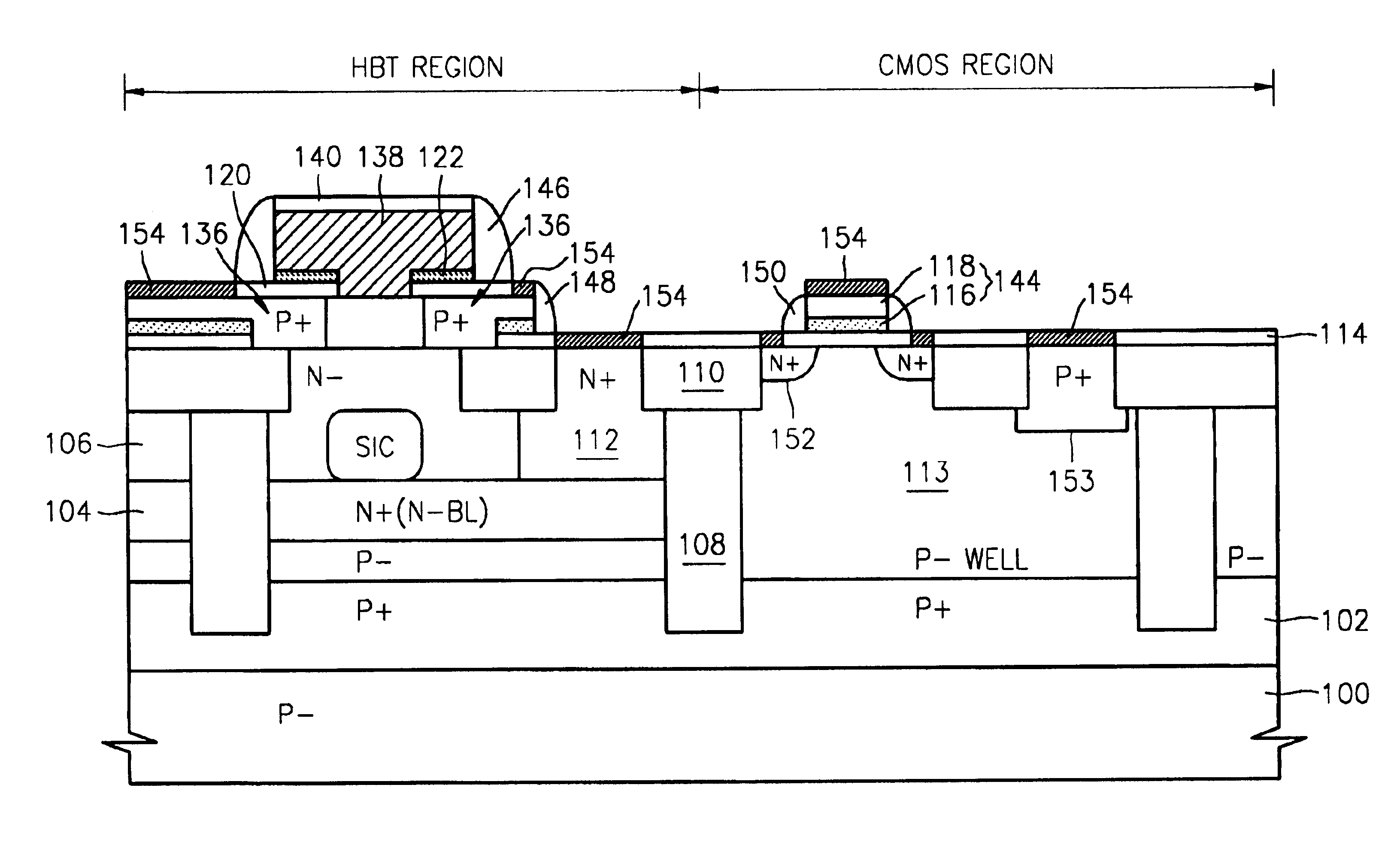
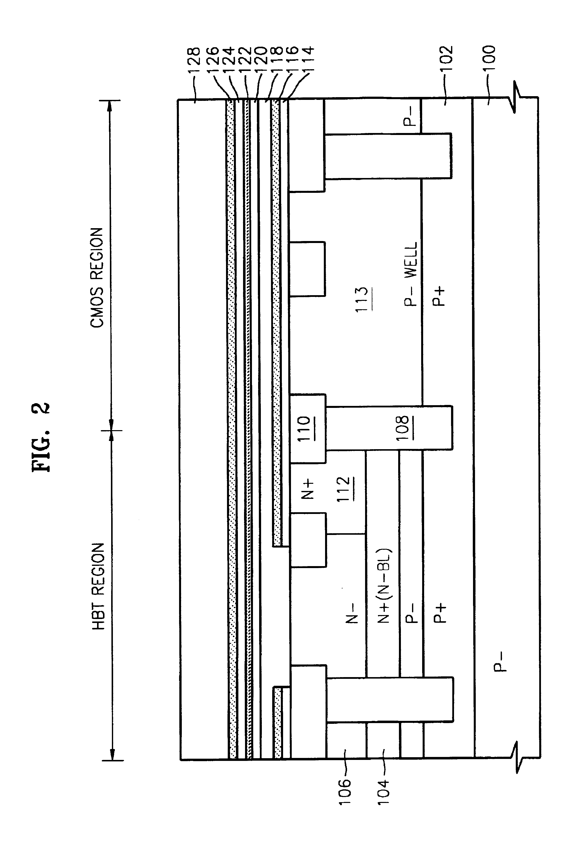
As described above, maintaining a high yield of high-frequency operation devices without degrading performance is essential to a SiGe HBT BiCMOS process. In the present invention, the following process is employed to stably reproduce emitter-base junctions, and variation of SICs is eliminated to improve reproducibility of base-collector junctions. Also, an extrinsic base, which is required to increase fMAX or reduce figure of noise, is formed in a self-aligned fashion in order to improve process reproducibility. The entire fabrication process is as follows.

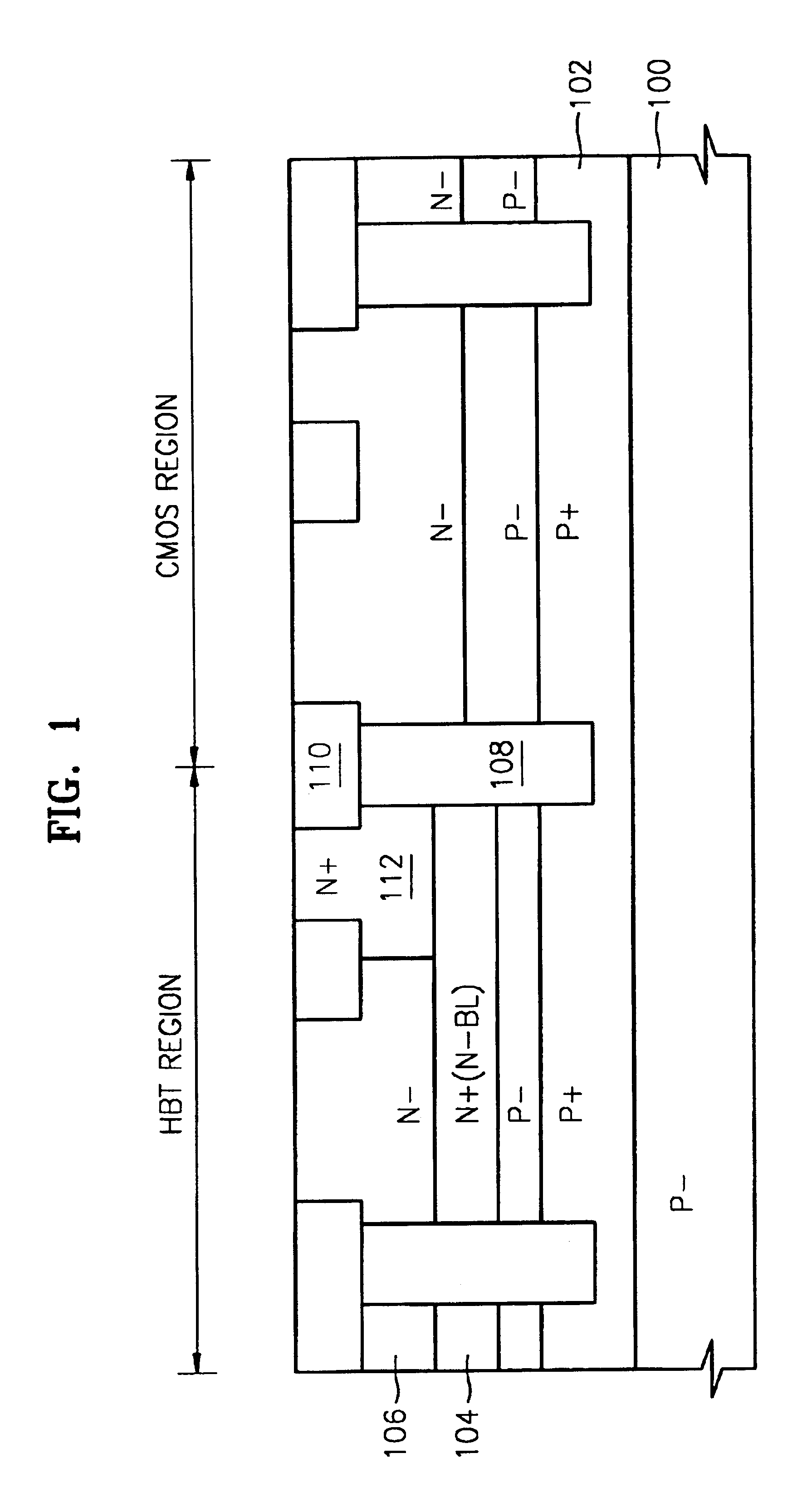
Referring to FIG. 1, a semiconductor substrate 100 including p−-type impurity ions, for example, a p−-type silicon substrate, is prepared. P+-type impurity ions are implanted into the p−-type semiconductor substrate 100 to form a p+-type region 102. Afterwards, n+-type impurity ions, such as As and P, are implanted into an HBT region by using a mask having a predetermined opening. Thus, a buried collector layer 104 (N-BL) is forme...


PUM


Abstract

Provided is a method for manufacturing a self-aligned BiCMOS including a SiGe heterojunction bipolar transistor (HBT) for performing high-frequency operations. In this method, an extrinsic base and a selective ion-implanted collector (SIC) are formed by a self-alignment process.

Description

CROSS REFERENCES TO RELATED APPLICATIONSThis application claims the priority of Korean Patent Application No. 2003-07870, filed on Feb. 7, 2003, the contents of which are incorporated herein by reference in their entirety.BACKGROUND OF THE INVENTION1. Field of the InventionThe present invention relates to a method for manufacturing a heterojunction bipolar transistor (HBT), and more particularly, to a method for manufacturing a BiCMOS by combining a process of manufacturing an HBT and a process of manufacturing a complementary metal oxide semiconductor (CMOS) transistor.2. Description of the Related ArtLaborious research into high-frequency operation transistors has progressed along with developments in high-speed communications technologies. In recent years, a SiGe HBT has been applied to high-frequency operation transistors. The SiGe HBT is different from a typical bipolar transistor in that a SiGe epitaxial layer forms a base. When SiGe, which has an energy bandgap that is smalle...

Claims


Application Information

Patent Timeline
Patent Type & Authority Patents(United States)
IPC IPC(8): H01L21/70H01L21/8249H01L21/8222H01L21/8248H01L21/331H01L27/04H01L27/06H01L29/737
CPCH01L21/8249H01L27/04
Inventor YI, SANG-DONSHIN, HEON-JONG
Owner SAMSUNG ELECTRONICS CO LTD
Why Eureka
Try Eureka