
Semiconductor device with stacked semiconductor elements

a semiconductor element and semiconductor technology, applied in the field of semiconductor devices, can solve problems such as the increase of demand

Inactive Publication Date: 2005-02-22
RENESAS ELECTRONICS CORP
View PDF3 Cites 13 Cited by
  • Summary
  • Abstract
  • Description
  • Claims
  • Application Information

AI Technical Summary

Problems solved by technology

However, although a conventional semiconductor device may not require an expensive multi-layer substrate for assembling by making the upper semiconductor element guide the electrical signals from the lower semiconductor element, an optimal pad layout or wiring method of easily assembling semiconductor elements having pads on two facing sides, whose demand has been increased, in packages having electrodes on four outer circumferential sides, such as QFP, cannot be known from this technique.

Method used


Image

  • Semiconductor device with stacked semiconductor elements
  • Semiconductor device with stacked semiconductor elements
  • Semiconductor device with stacked semiconductor elements

Examples


first embodiment

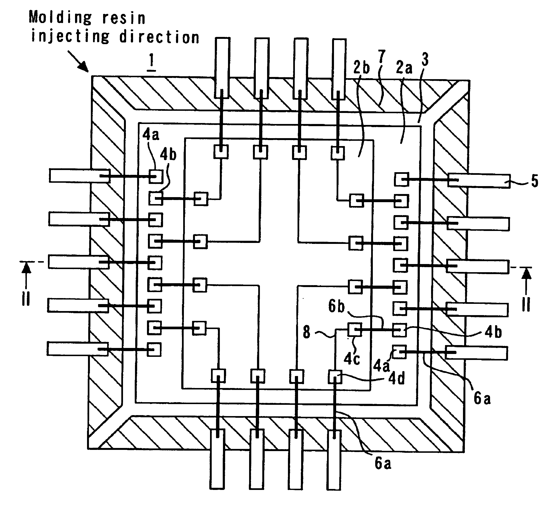
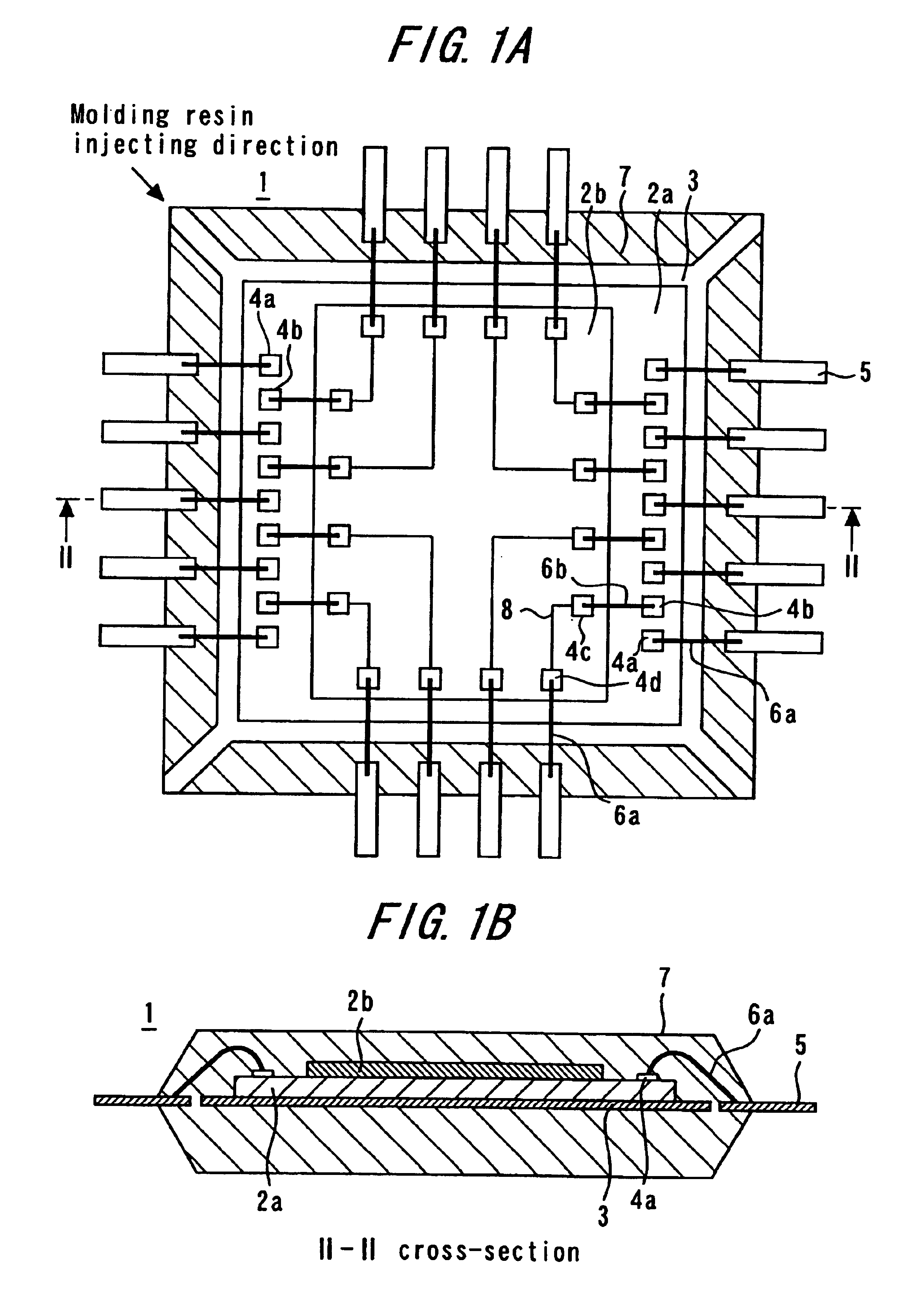
FIG. 1A is a plan showing a semiconductor device according to a First Embodiment of the present invention whose upper portion of a molding resin is cut away; and FIG. 1B is a cross-section thereof along a chain line II—II. In the drawings, reference numeral 1 denotes a semiconductor device. A first semiconductor element 2a has a plurality of first pads 4a and a plurality of second pads 4b arrayed along the two facing sides of the major surface. A second semiconductor element 2b has a plurality of third pads 4c and a plurality of fourth pads 4d. The plurality of third pads 4c are arrayed along sides where the first pads 4a and the second pads 4b are arrayed. The plurality of fourth pads 4d are arrayed along sides where the first pads 4a and the second pads 4b are not arrayed. Aluminum wirings 8 are first wirings for electrically connecting the plurality of third pads 4c to the plurality of fourth pads 4d on the major surface. The aluminum wirings 8 are formed in an interlayer film (n...

second embodiment

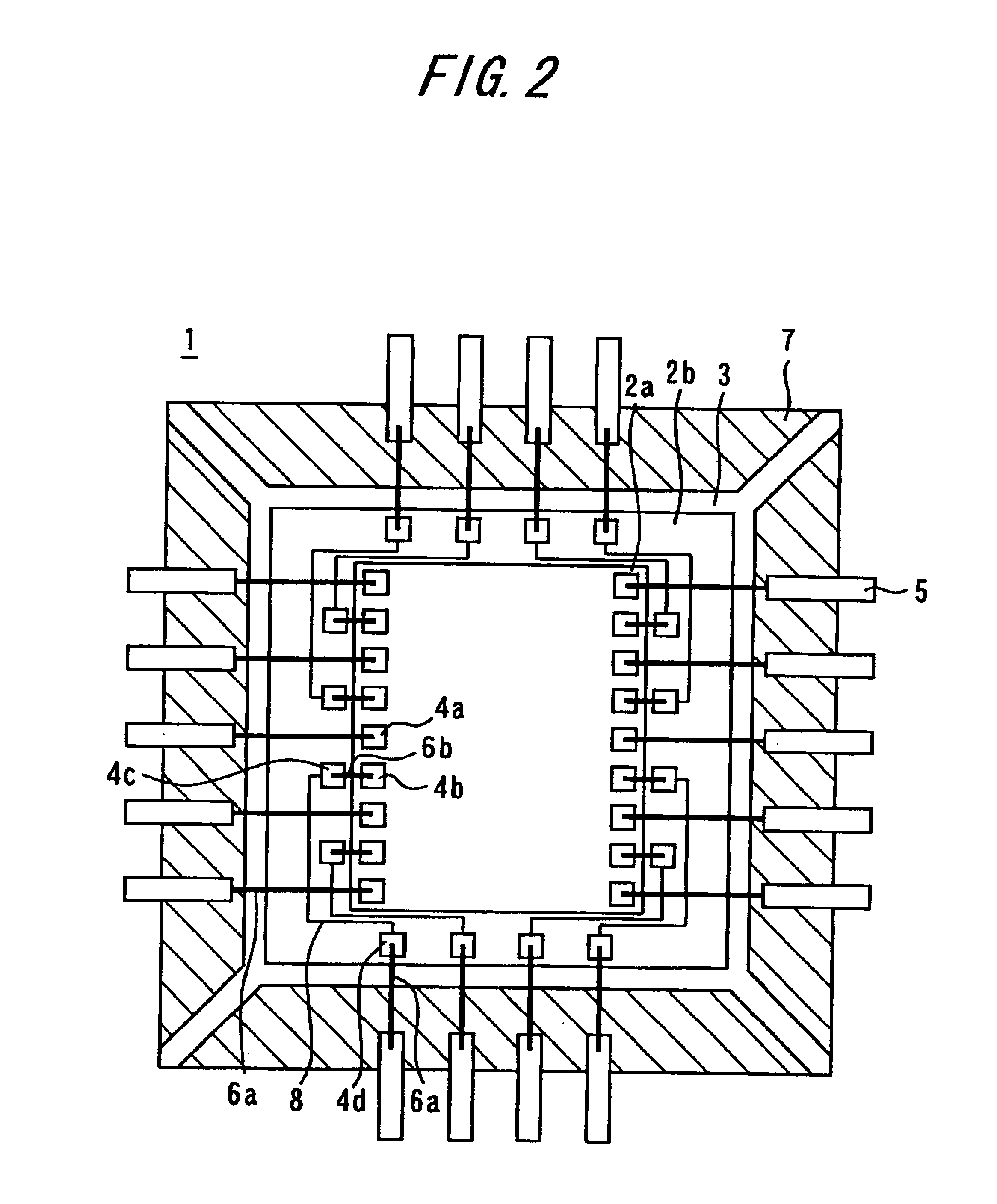
FIG. 2 is a perspective plan showing a semiconductor device according to a Second Embodiment of the present invention whose upper portion of the molding resin is cut away. The parts same as or corresponding to the parts in FIG. 1 are denoted by the same reference numerals, and the description thereof will be omitted. The semiconductor device 1 of the First Embodiment has a second semiconductor element 2b stacked on a first semiconductor element 2a, while the semiconductor device 1 of the Second Embodiment has a first semiconductor element 2a stacked on a second semiconductor element 2b. By adopting this structure, the connection of the pads 4b of the first semiconductor element 2a to the inner leads 5 can be realized through the second semiconductor element 2b even if the second semiconductor element 2b has a larger area than that of the first semiconductor element 2a.

third embodiment

FIG. 3 is a perspective plan showing a semiconductor device according to a Third Embodiment of the present invention whose upper portion of the molding resin is cut away. The parts same as or corresponding to the parts in FIG. 1 are denoted by the same reference numerals, and the description thereof will be omitted. The semiconductor device 1 of the Third Embodiment has two rows of pads 4a and pads 4b on each of two facing sides of a semiconductor element 2a. By adopting this structure, a larger number of pads 4a and pads 4b can be provided on a semiconductor element without damaging easiness of probing in wafer test. Furthermore, three or more rows of pads 4a and pads 4b may be disposed on each side, and thereby, the number of pads that can be disposed can be increased.


PUM


Abstract

In a semiconductor device 1, a substrate 3 carries the first semiconductor element 2a and the second semiconductor element 2b. The first semiconductor element 2a has a plurality of first pads 4a and a plurality of second pads 4b arrayed along two facing sides of a major surface. The second semiconductor element 2b has a plurality of third pads 4c along sides where the first pads 4a and the second pads 4b are arrayed, and a plurality of fourth pads 4d along sides where the first pads 4a and the second pads 4b are not arrayed. First wirings 8 electrically connect the plurality of third pads 4c to the plurality of fourth pads 4d on the major surface. A plurality of electrodes 5 is arrayed along all the circumferential sides of the major surface of the substrate 3. Second wirings 6a electrically connect the plurality of first pads 4a and the plurality of fourth pads 4d respectively to the plurality of electrodes 5. Third wirings 6b electrically connect the plurality of second pads 4b to the plurality of third pads 4c.

Description

BACKGROUND OF THE INVENTION1. Field of the InventionThe present invention relates to a semiconductor device that can easily assemble semiconductor elements having pads arrayed along two facing sides of the major surface in a package having electrodes arrayed along all the outer circumferential sides of the major surface of a substrate whereon the semiconductor elements are placed.2. Background ArtIn a conventional semiconductor device having a stacked MCM structure, a dummy wiring is formed on an upper semiconductor element, and the electrical signals from a lower semiconductor element are communicated through the dummy wiring to a lead, which is a terminal for external connection. Thereby, the electrical signals from a lower semiconductor element can be guided by the upper semiconductor element (refer to e.g., Japanese Patent Laid-Open No. 11-220091 (pp. 1-4, FIGS. 1-6)).For the purpose of the reduction of the area of a semiconductor element due to the optimization of a pad arrange...

Claims


Application Information

Patent Timeline
Patent Type & Authority Patents(United States)
IPC IPC(8): H01L23/31H01L23/495H01L23/28H01L25/065H01L23/48H01L25/18H01L25/07
CPCH01L23/3128H01L24/49H01L25/0657H01L23/49575H01L2225/06568H01L24/45H01L2224/45144H01L2224/48091H01L2224/48227H01L2224/48247H01L2224/49175H01L2924/01004H01L2924/01005H01L2924/01006H01L2924/01013H01L2924/01079H01L2924/01082H01L2924/15311H01L2225/06506H01L2225/0651H01L2924/014H01L2924/01033H01L24/48H01L2924/00014H01L2924/00H01L2924/181H01L2224/05554H01L2924/10162H01L2224/023H01L2924/0001
Inventor HATAUCHI, KAZUSHI
Owner RENESAS ELECTRONICS CORP
Learn More