Wafer level phosphor coating method and devices fabricated utilizing method

a phosphor coating and wafer level technology, applied in semiconductor devices, semiconductor/solid-state device details, electrical devices, etc., can solve the problems of difficult to consistently reproduce leds with the same or similar emission characteristics, difficult to control the geometry and thickness of the phosphor layer, and non-uniform color temperatur

Active Publication Date: 2008-07-24
CREELED INC
View PDF101 Cites 799 Cited by
  • Summary
  • Abstract
  • Description
  • Claims
  • Application Information

AI Technical Summary

Problems solved by technology

Using this method, however, it can be difficult to control the phosphor layer's geometry and thickness.
As a result, light emitting from the LED at different angles can pass through different amounts of conversion material, which can result in an LED with non-uniform color temperature as a function of viewing angle.
Because the geometry and thickness is hard to control, it can also be difficult to consistently reproduce LEDs with the same or similar emission characteristics.
Like the syringe method above, using the stencil method can be difficult to control the geometry and layer thickness of the phosphor containing polymer.
The stenciling composition may not fully fill the stencil opening such that the resulting layer is not uniform.
These problems can result in LEDs having non-uniform color temperature and LEDs that are difficult to consistently reproduce with the same or similar emission characteristics.
With these approaches the key challenge is accessing the wire bond pad on the device after the coating process.
Accessing the wire bond by standard wafer fabrication techniques is difficult with typical silicone binding material, as well as other binder materials such as epoxies or glass.
Silicones are not compatible with commonly used wafer fabrication materials such as acetone, as well as some developers, and resist strippers.
This can limit the options and choices for the particular silicones and process steps.
Cured silicone films with phosphor are also difficult to etch and have a very slow etch rate in chlorine and CF4 plasma, and wet etching of cured silicones is typically inefficient.

Method used


Image

  • Wafer level phosphor coating method and devices fabricated utilizing method
  • Wafer level phosphor coating method and devices fabricated utilizing method
  • Wafer level phosphor coating method and devices fabricated utilizing method

Examples


Embodiment Construction

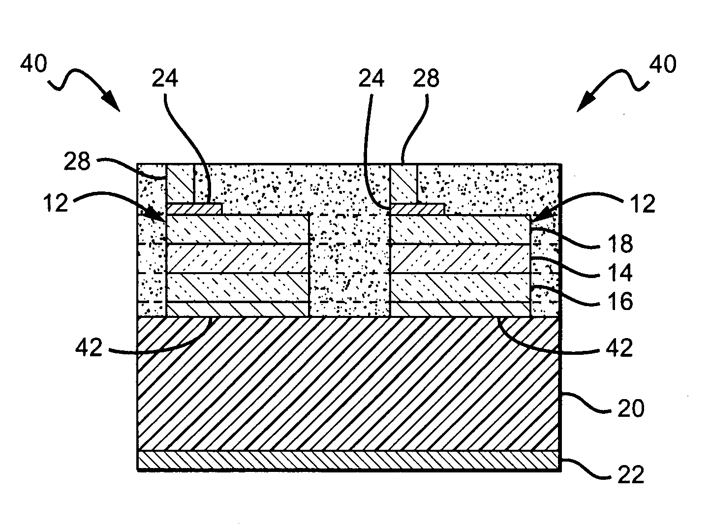
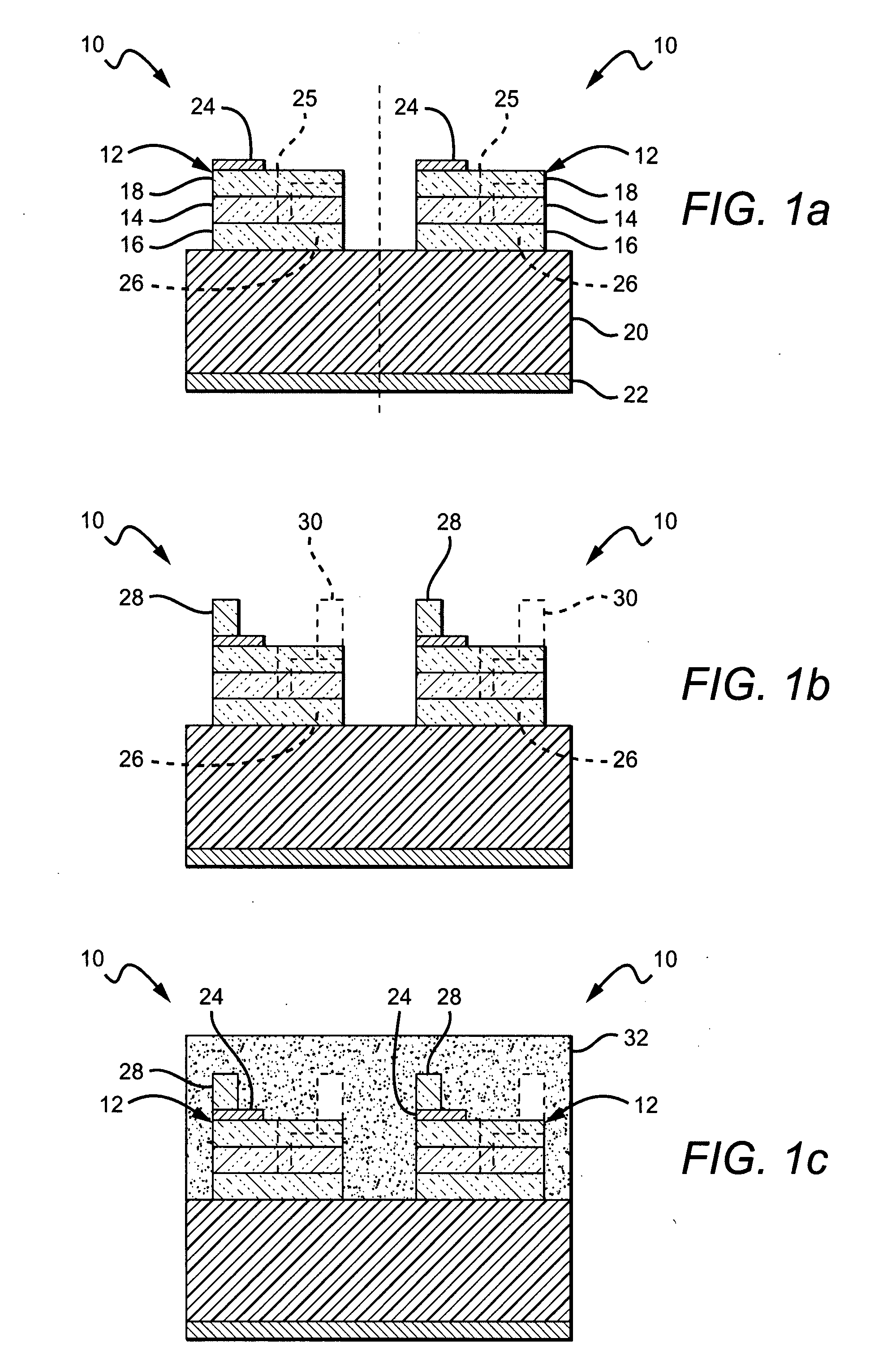
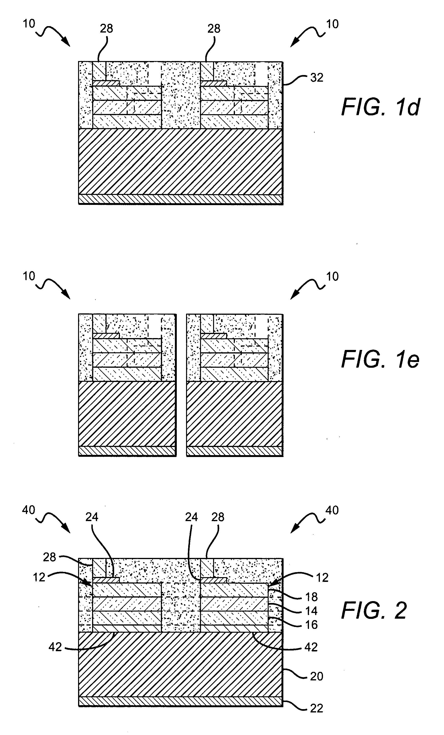
[0032]The present invention provides fabrication methods that are particularly applicable to wafer level coating of semiconductor devices such as LEDs. The present invention also provides semiconductor devices, such as LEDs fabricated using these methods. The present invention allows coating of LEDs at the wafer level with a down-converter layer (e.g. phosphor loaded silicone) while still allowing access to one or more of the contacts for wire bonding. According to one aspect of the present invention, electrically conducting pedestals / posts are formed on one or both of the LED contacts (bond pads) while the LEDs are at the wafer level. These pedestals can be fabricated using known techniques such as electroplating, electroless plating, stud bumping, or vacuum deposition. The wafer can then be blanket coated with a down-converter coating layer, burying the LEDs, contacts and pedestals. Each of the pedestals act as a vertical extension of its contact, and although the blanket coating ...


PUM

PropertyMeasurementUnit
temperatureaaaaaaaaaa
thicknessaaaaaaaaaa
thicknessaaaaaaaaaa

Abstract

Methods for fabricating light emitting diode (LED) chips comprising providing a plurality of LEDs typically on a substrate. Pedestals are deposited on the LEDs with each of the pedestals in electrical contact with one of the LEDs. A coating is formed over the LEDs with the coating burying at least some of the pedestals. The coating is then planarized to expose at least some of the buried pedestals while leaving at least some of said coating on said LEDs. The exposed pedestals can then be contacted such as by wire bonds. The present invention discloses similar methods used for fabricating LED chips having LEDs that are flip-chip bonded on a carrier substrate and for fabricating other semiconductor devices. LED chip wafers and LED chips are also disclosed that are fabricated using the disclosed methods.

Description

[0001]This invention was made with Government support under Contract USAF 05-2-5507. The Government has certain rights in this inventionBACKGROUND OF THE INVENTION[0002]1. Field of the Invention[0003]This invention relates to methods for fabricating semiconductor devices and in particular methods for wafer level coating of light emitting diodes.[0004]2. Description of the Related Art[0005]Light emitting diodes (LED or LEDs) are solid state devices that convert electric energy to light, and generally comprise one or more active layers of semiconductor material sandwiched between oppositely doped layers. When a bias is applied across the doped layers, holes and electrons are injected into the active layer where they recombine to generate light. Light is emitted from the active layer and from all surfaces of the LED.[0006]Conventional LEDs cannot generate white light from their active layers. Light from a blue emitting LED has been converted to white light by surrounding the LED with a...

Claims


Application Information

Patent Timeline
Patent Type & Authority Applications(United States)
IPC IPC(8): H01L33/00H01L33/38H01L33/44H01L33/50H01L33/62
CPCH01L23/3114H01L33/38H01L33/44H01L33/508H01L33/62H01L2933/0041H01L2924/0002H01L33/387H01L33/507H01L33/501H01L2924/00
Inventor CHITNIS, ASHAYIBBETSON, JAMESCHAKRABORTY, ARPANTARSA, ERIC J.KELLER, BERNDSERUTO, JAMESFU, YANKUN
Owner CREELED INC
Why Eureka
Try Eureka