Three-dimensional chip stacking assembly

a three-dimensional chip and assembly technology, applied in the direction of basic electric elements, electrical apparatus, semiconductor devices, etc., can solve the problems of inability to achieve high-level 3d integration. achieve the effect of good mechanical and thermal integrity and precise alignmen

Inactive Publication Date: 2002-03-12
IBM CORP
View PDF5 Cites 751 Cited by
  • Summary
  • Abstract
  • Description
  • Claims
  • Application Information

AI Technical Summary

Benefits of technology

It is a further object of the invention to stack the chips while maintaining a precise alignment between all the chips forming the stack

Problems solved by technology

Furthermore, the processes involved in forming successively devices can affect the characteristics of devices placed underneath it.
In addition, the total fabrication time and complexity is proportional to the number of layers, and becomes impractical for higher levels of 3D integration.
A typical technique of forming a 3D-IC assembly by stacking silicon-on-insulator (SOI) wafers, but using a temporary silicon substrate, is described, e.g., in U.S. Pat. No. 5,426,072 to Finnila. are several problems associated with stacking wafers.
First, the yield loss is very large.
A low yield forcibly resul

Method used


Image

  • Three-dimensional chip stacking assembly
  • Three-dimensional chip stacking assembly
  • Three-dimensional chip stacking assembly

Examples


Embodiment Construction

Having by now described the wafer preparation process, the chip alignment and the attachment process applicable to a multi-layer chip stacking technology will be described hereinafter. This description will then be followed by an illustrative example.
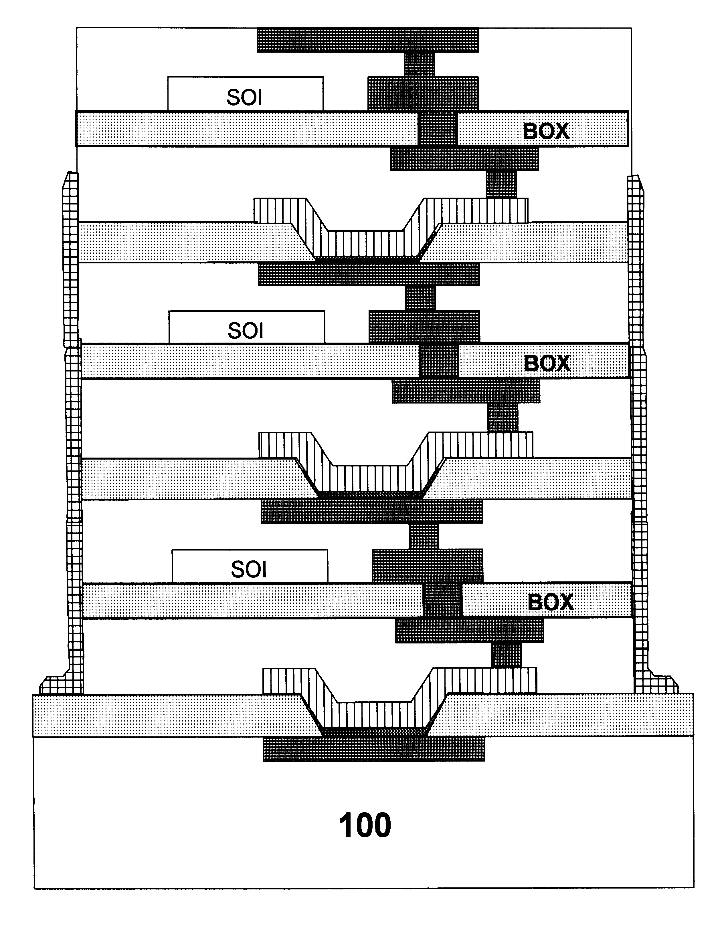
Chip Stacking

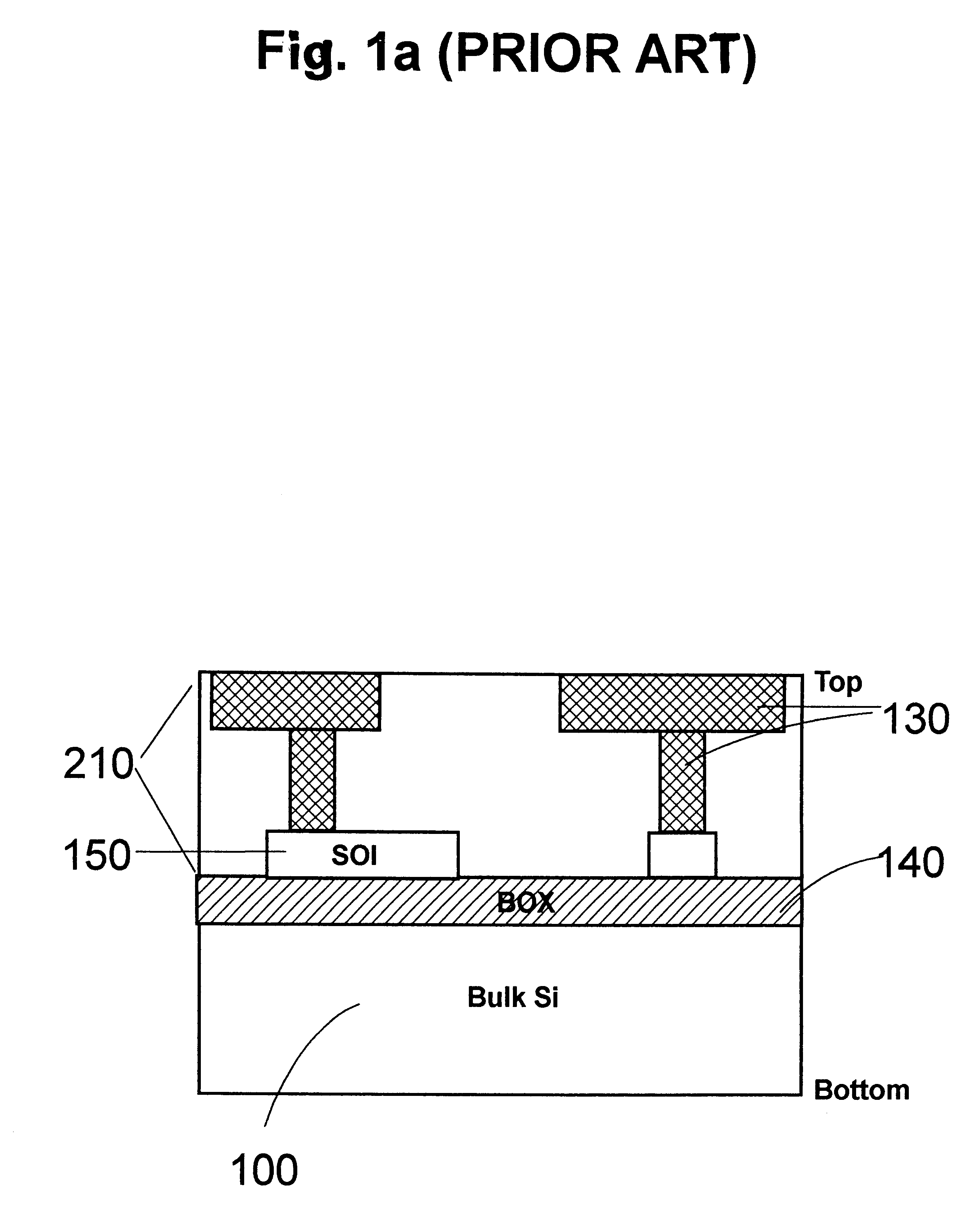
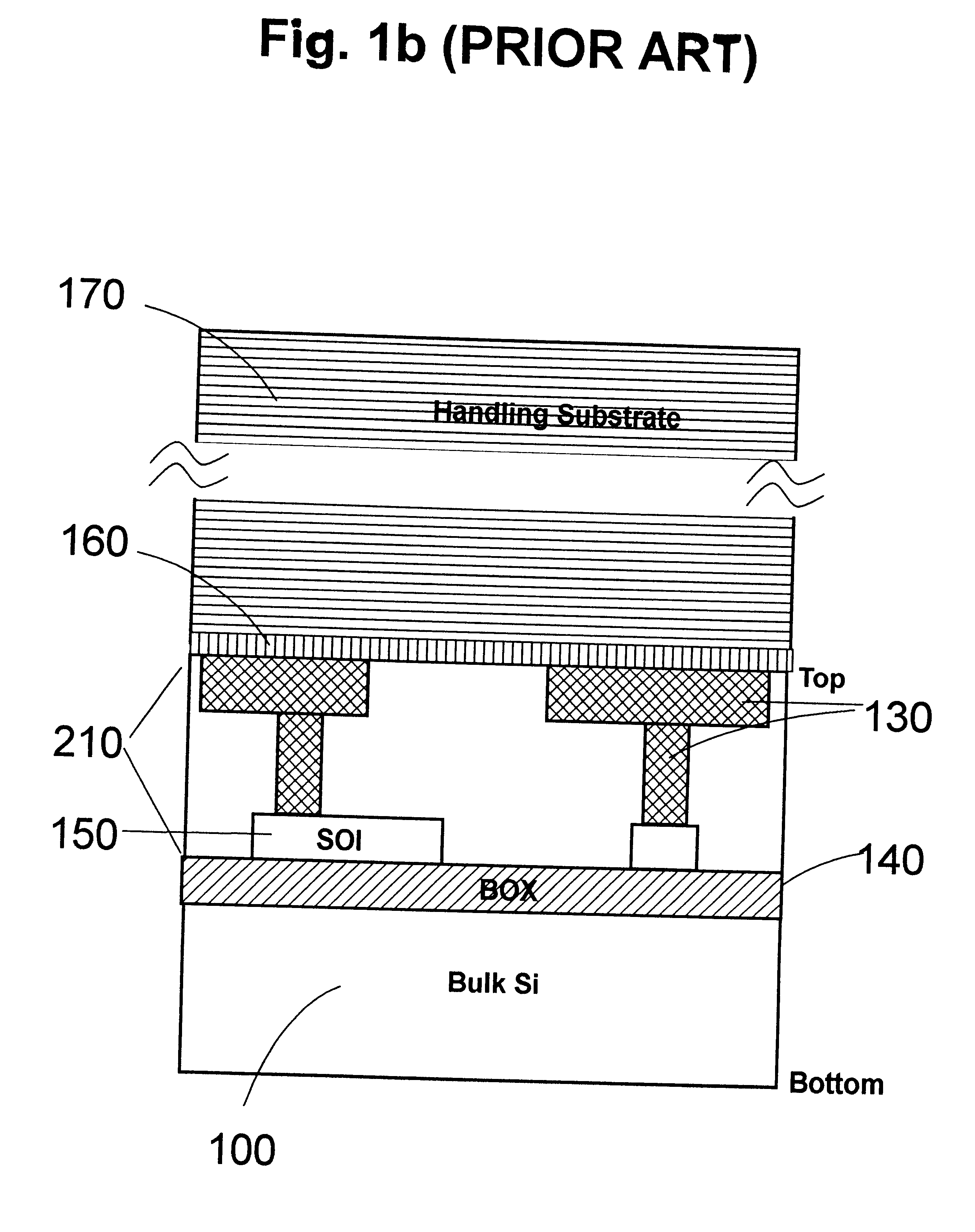
Referring to FIG. 2, there is shown an SOI wafer having a handling substrate (170), frontside interconnection layers (210) and backside interconnection layers (220), as shown previously with reference to FIG. 1, with the SOI wafer now diced into individual chips (225). Wafer level testing can be performed prior to dicing in order to screen out defective chips.

In FIG. 3, the individual chips are mounted, an operation that requires aligning the chips and attaching them to a substrate (100). As previously stated, the substrate is either an SOI / bulk chip, SOI / bulk wafer or thin-film substrate. In all cases, they are provided with appropriate alignment patterns (240, 250) for alignment purposes and other joint structures (260, 2...


PUM


Abstract

An assembly consisting of three dimensional stacked SOI chips, and a method of forming such integrated circuit assembly, each of the SOI chips including a handler making mechanical contact to a first metallization pattern making electrical contact to a semiconductor device. The metalized pattern, in turn, contacts a second metallization pattern positioned on an opposite surface of the semiconductor device. The method of fabricating the three-dimensional IC assembly includes the steps of: a) providing a substrate having a third metalized pattern on a first surface of the substrate; b) aligning one of the SOI chips on the first surface of the substrate, by having the second metallization pattern of the SOI chip make electrical contact with the third metalized pattern of the substrate; c) removing the handler from the SOI chip, exposing the first metallization pattern of the SOI chip; d) aligning a second one of the SOI chips with the first SOI chip, having the second metallization pattern of the second SOI chip make electrical contact to the exposed first metallization pattern of the first SOI chip; and e) repeating steps c) and d) for mounting subsequent SOI chips one on top of the other.

Description

This invention is generally related to the fabrication of a three-dimensional integrated circuit (IC) chip or wafer assembly, and more particularly to a method of stacking ultra-thin chips with interconnections designed to maximize the speed of the overall IC package.Three-dimensional integrated circuits (3D-IC) have proven to be the favored approach for improving the performance of semiconductor products. Density can be upgraded many fold by stacking chips or wafers. Significant speed improvement can also be expected because the interconnecting wires linking the chips are shortened substantially.Several techniques for achieving 3D-IC configurations have been used in the past. One approach utilizes a fabrication technology wherein active silicon films are grown in successive layers with intervening insulation layers. However, this approach must overcome many problems related to the materials used. Furthermore, the processes involved in forming successively devices can affect the cha...

Claims


Application Information

Patent Timeline
IPC IPC(8): H01L21/70H01L25/065H01L21/98H01L21/68H01L21/67H01L21/768H01L21/84
CPCH01L24/81H01L25/0657H01L25/50H01L21/84H01L21/6835H01L2924/014H01L2221/6835H01L2221/68359H01L2221/68368H01L2224/81001H01L2224/81121H01L2224/81801H01L2225/06513H01L2225/06541H01L2924/01013H01L2924/01029H01L2924/01082H01L2924/10329H01L2924/01005H01L2924/01006H01L2924/01019H01L2924/01033H01L2924/01074H01L2224/05571H01L2224/16145H01L2224/81815H01L2224/81141H01L2224/16237H01L2924/14H01L2924/00012H01L2924/00H01L21/768
Inventor FUNG, KA HINGPOGGE, H. BERNHARD
Owner IBM CORP
Why Eureka
Try Eureka