
Surface acoustic wave devices based on unpolished nanocrystalline diamond

a nanocrystalline diamond and surface acoustic wave technology, applied in piezoelectric/electrostrictive devices, piezoelectric/electrostrictive/magnetostrictive devices, piezoelectric/electrostriction/magnetostriction machines, etc., can solve the problem that the limits of conventional photolithography are pushed to the limit by multiple pairs per wavelength and higher resonant frequencies, so as to achieve more sensitive effects

Inactive Publication Date: 2005-02-22
MICHIGAN STATE UNIV BOARD OF TRUSTEES OPERATING
View PDF23 Cites 16 Cited by
  • Summary
  • Abstract
  • Description
  • Claims
  • Application Information

AI Technical Summary

Problems solved by technology

More complex designs with multiple pairs per wavelength and higher resonant frequencies tend to push the limits of conventional photolithography.

Method used


Image

  • Surface acoustic wave devices based on unpolished nanocrystalline diamond
  • Surface acoustic wave devices based on unpolished nanocrystalline diamond
  • Surface acoustic wave devices based on unpolished nanocrystalline diamond

Examples


Embodiment Construction

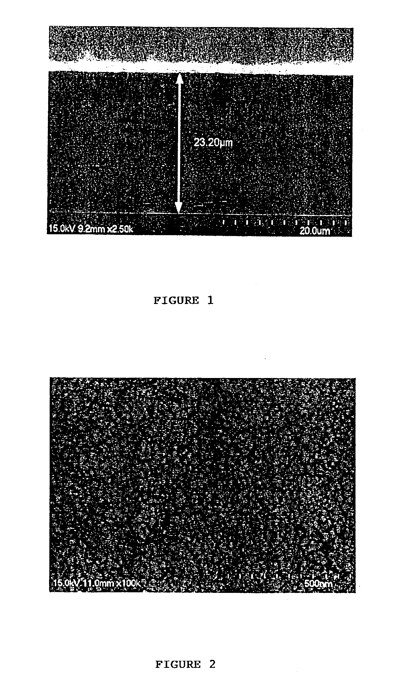
canning electron micrograph of the growth surface of a nanocrystalline diamond film used for surface acoustic wave device studies.

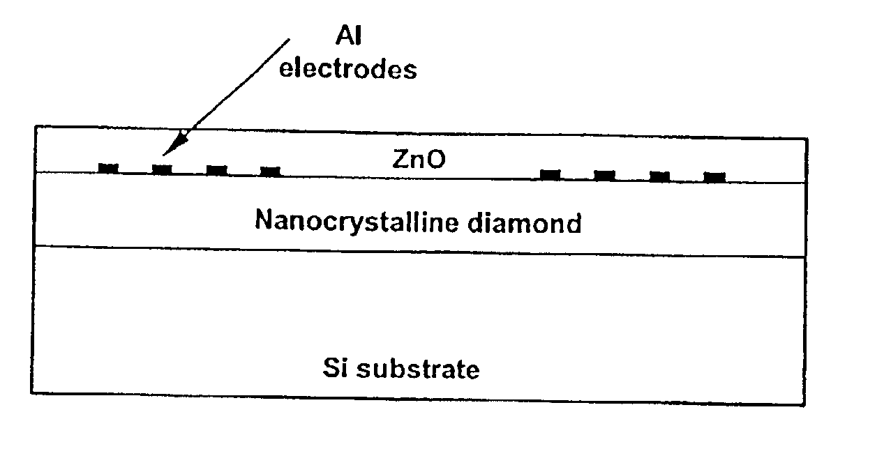
[0027]FIG. 3 is a schematic cross-sectional diagram of the surface acoustic wave device multilayer structure (not to scale).

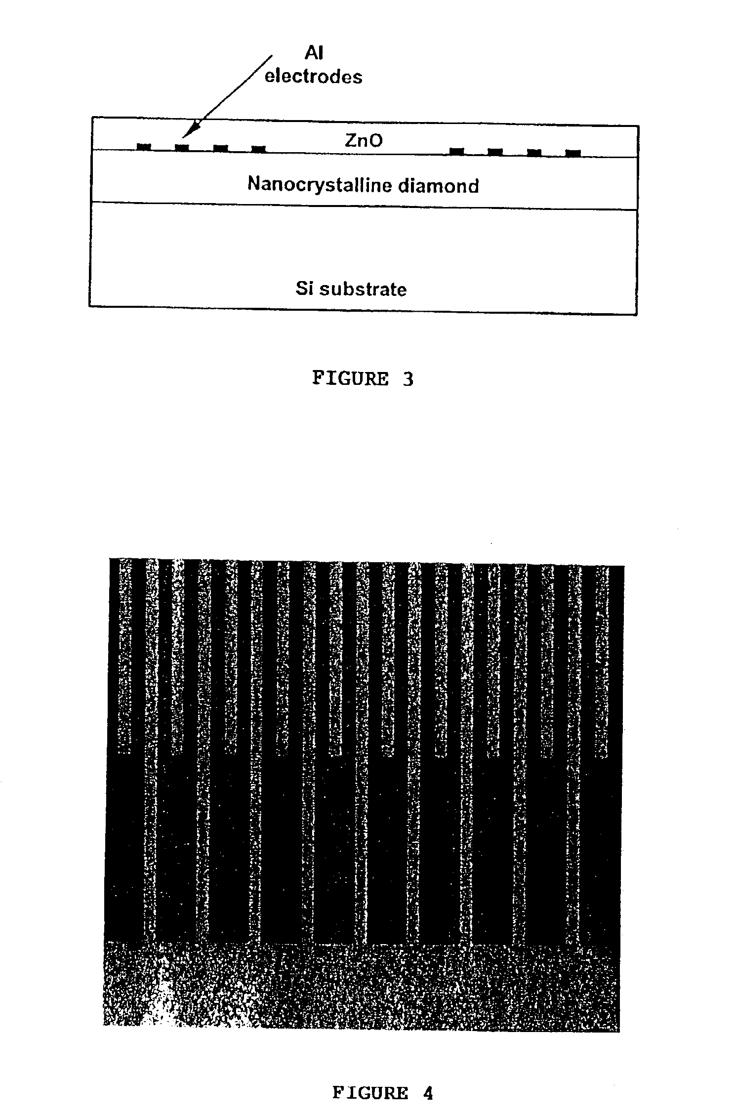
[0028]FIG. 4 is an optical micrograph of Al interdigitated electrodes on the as-grown surface of nanocrystalline diamond. The lateral dimension of each electrode finger is 3 μm.

[0029]FIG. 5 is a graph showing phase velocities as measured for surface waves on nanocrystalline diamond (□) and on large-grain polished polycrystalline diamond (∘). Here, k is the wave vector (2π / λ, where λ is the wavelength of sound in ZnO). The solid lines represent calculations of phase velocities based on single crystal diamond material parameters. The labels denote the Rayleigh mode indices for the layered medium. The dashed line shows the Rayleigh wave velocity on ZnO.

DESCRIPTION OF PREFERRED EMBODIMENTS

[0030]Surface acoustic wave (SAW) devices based o...


PUM

PropertyMeasurementUnit
temperatureaaaaaaaaaa
pressureaaaaaaaaaa
pressureaaaaaaaaaa

Abstract

Surface Acoustic Wave (SAW) devices with an unpolished or nominally polished nanocrystalline diamond film, metal electrodes and piezoelectric composition coatings are described. The devices are used as radio frequency and microwave filters.

Description

CROSS-REFERENCE TO RELATED APPLICATIONS[0002]This application claims priority to Provisional application Ser. No. 60 / 351,955, filed Jan. 25, 2002.GOVERNMENT RIGHTS[0003]The present invention was developed under National Science Foundation Grant DMR-9809688. The U.S. Government may have certain rights to the present invention.BACKGROUND OF THE INVENTION[0004](1) Field of the Invention[0005]The present invention relates to surface acoustic wave (SAW) and bulk acoustic wave (BAW) devices with unpolished nanocrystalline diamond which supports the surface acoustic wave. In particular the nanocrystalline diamond is composed of individual grains roughly between 1 nm and 50 nanometers. This material is also referred to as ultra-nanocrystalline diamond (UNCD).[0006](2) Description of Related Art[0007]Bulk acoustic wave devices are also known. These find use as filters and in sensors. In general diamond is surrounded by one or more piezoelectric films or plates.[0008]SAW devices function as t...

Claims


Application Information

Patent Timeline
Patent Type & Authority Patents(United States)
IPC IPC(8): H03H9/02
CPCH03H9/02582
Inventor BI, BAOKANGGOLDING, BRAGEHUANG, WEN-SHINASMUSSEN, JES
Owner MICHIGAN STATE UNIV BOARD OF TRUSTEES OPERATING
Learn More