Formation of dual work function gate electrode

a dual-function, gate electrode technology, applied in the direction of basic electric elements, semiconductor/solid-state device manufacturing, electrical equipment, etc., can solve the problems of difficult formation of p-type doped gate electrodes, inability to obtain uniform gate uniformity, and extremely difficult critical dimension of gates, etc., to achieve the effect of reducing boron penetration and eliminating boron depletion

Inactive Publication Date: 2005-03-15
POLARIS INNOVATIONS LTD
View PDF7 Cites 2 Cited by
  • Summary
  • Abstract
  • Description
  • Claims
  • Application Information

AI Technical Summary

Benefits of technology

Another object of the present invention is to provide a process for making a dual work function gate electrode CMOS semiconductor structure with p-type doped electrodes wherein, during the manufacturing process, there is substantial suppression of boron penetration onto the channel region without depletion of boron near the gate oxide.

Problems solved by technology

However, due to the fact that the surface of the layer formed by the large grain poly-silicon is rough because of the size of the grain, UV exposure light is scattered upon patterning the poly-silicon layer to form gates.
Unfortunately, when this happens, the critical dimension of the gate is extremely difficult to control and uniformity of the gate cannot be obtained.
In the aggressive scaling of CMOS devices to smaller feature sizes wherein there is the requirement of the use of surface-channel pMOSFET to minimize the short-channel effect to improve device performance, wherein a p-type doped gate electrodes must inevitably be used to realize the surface-channel pMOSFET, and wherein formation of p-type doped gate electrodes is very difficult due to severe boron penetration into the channel region during subsequent high-thermal processes, and wherein to suppress boron penetration low thermal processing is required but leads to boron depletion near the gate oxide, there is a need to devise a process wherein a p-type doped gate electrode may be formed without boron penetration into the channel region and without boron depletion near the gate oxide.

Method used


Image

  • Formation of dual work function gate electrode
  • Formation of dual work function gate electrode
  • Formation of dual work function gate electrode

Examples


Embodiment Construction

As mentioned, the invention process is a method of forming CMOS structures of p-type doped gate electrodes without boron penetration into the channel region and without boron depletion near the gate oxide region using laser annealing at an energy level sufficient to melt at least a portion of a-Si but insufficient to melt the poly-Si.

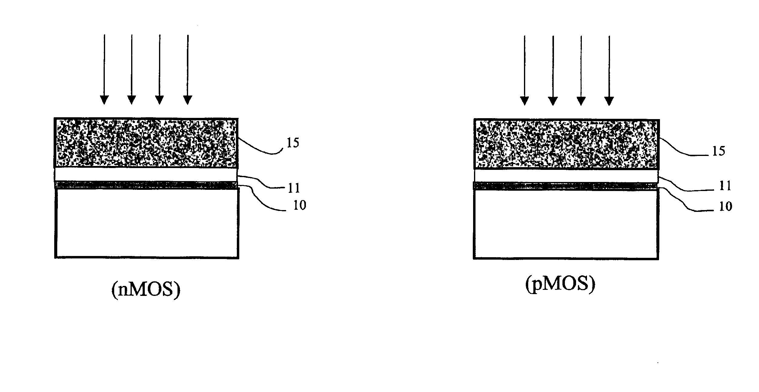
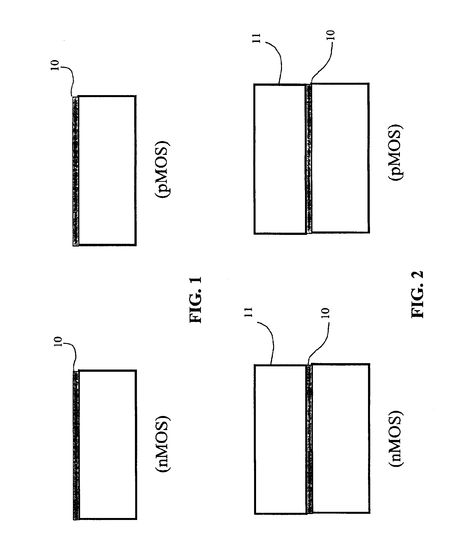
In this regard, reference is now made to FIG. 1 which depicts a simplified cross sectional configuration of a CMOS showing the step of gate oxidation over a channel for a nMOS transistor and over a channel of a pMOS transistor, in the formation of a dual work function gate electrode using bi-layer (a-Si / poly-Si), implant, and laser annealing. The gate oxidation layer of oxide 10 is deposited on each nMOS and pMOS site. Thereafter, as may be seen in FIG. 2, an undoped poly-Si layer 11 is deposited on the oxide layer 10. Preferably, the undoped poly Si deposition is between 500˜3000 Å.

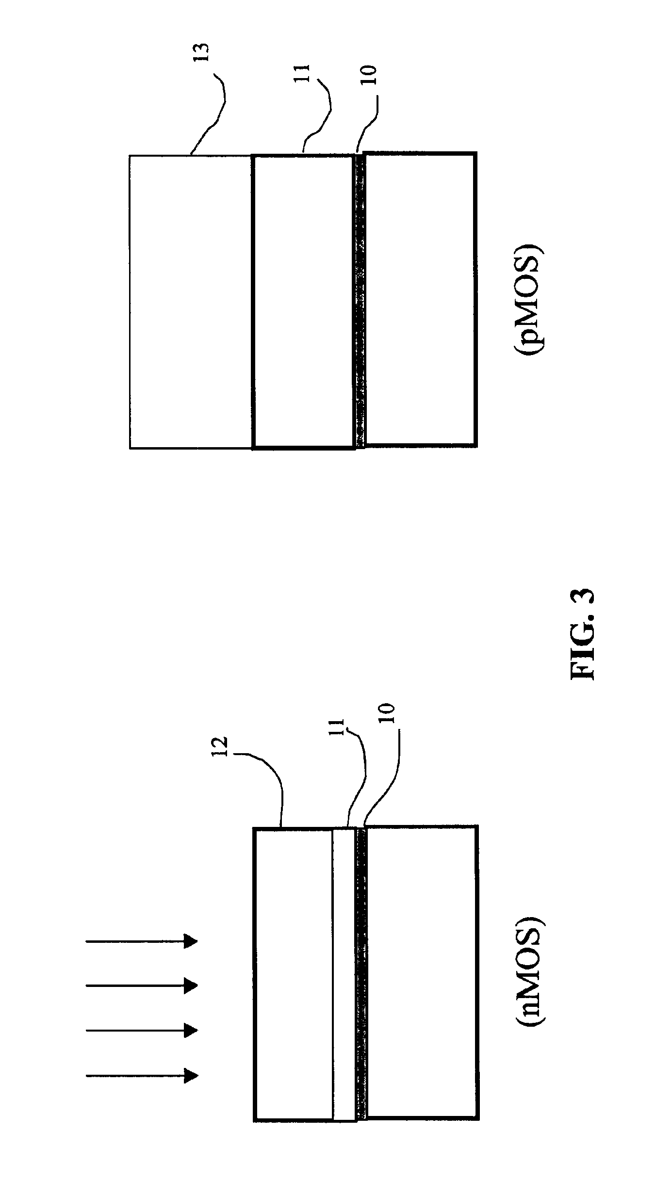
In FIG. 3 an amorphous silicon (a-Si) layer is next deposited by use of...


PUM


Abstract

In a method of making a dual work function gate electrode of a CMOS semiconductor structure, the improvement comprising formation of the dual work function gate electrode so that there is no boron penetration in the channel region and no boron depletion near the gate oxide, comprising:a) forming a gate oxide layer over a channel of a nMOS site and over a channel of a pMOS site;b) forming an undoped polysilicon layer over the gate oxide layer;c) masking the pMOS site, forming an a-Si layer over the nMOS site using a first heavy ion implantation, and implanting arsenic solely into the a-Si layer;d) masking the nMOS site formed by step c), forming an a-Si layer over the pMOS site using a second heavy ion implantation, and implanting boron solely into the a-Si regions;e) laser annealing the nMOS and pMOS sites for a short time and at an energy level sufficient to melt at least a portion of the a-Si but insufficient to melt the polysilicon; andf) affecting cooling after laser annealing to convert a-Si into polysilicon without gate oxide damage.

Description

BACKGROUND OF THE INVENTION1. Field of the InventionThe invention relates to a method for forming p-type doped gate electrodes during manufacture of CMOS semiconductor structures without boron penetration into the channel region and without boron depletion near the gate oxide.2. Description of The Related ArtIt is known that, in forming a gate on a substrate during manufacturing of a semiconductor device, large grain poly-silicon is used as the gate material. However, due to the fact that the surface of the layer formed by the large grain poly-silicon is rough because of the size of the grain, UV exposure light is scattered upon patterning the poly-silicon layer to form gates. Unfortunately, when this happens, the critical dimension of the gate is extremely difficult to control and uniformity of the gate cannot be obtained.To resolve this problem in the conventional method of manufacturing semiconductor devices, amorphous silicon (a-Si) is employed as the gate material on a substrat...

Claims


Application Information

Patent Timeline
Patent Type & Authority Patents(United States)
IPC IPC(8): H01L21/70H01L21/8238
CPCH01L21/823842
Inventor LEE, KILHOKANG, WOO-TANGRENGARAJAN, RAJESH
Owner POLARIS INNOVATIONS LTD
Why Eureka
Try Eureka