Layout method of semiconductor device

a semiconductor device and layout technology, applied in the direction of semiconductor devices, electrical devices, transistors, etc., can solve the problems of a potentially wide variance in process deviation at the gate of the transistor, the malfunction of the semiconductor device, and the variance of process deviation at the gate, so as to achieve the effect of minimizing the variance in process deviation

Inactive Publication Date: 2005-03-29
SAMSUNG ELECTRONICS CO LTD
View PDF9 Cites 133 Cited by
  • Summary
  • Abstract
  • Description
  • Claims
  • Application Information

AI Technical Summary

Benefits of technology

It is an object to provide a layout method of a semiconductor device to minimize t

Problems solved by technology

Some fabricating techniques for conventional semiconductor device, e.g., the uneven light reflection of the photo process and non-uniformity of the etching process, have brought about variances in process deviations at gates of transistors.
When it is not substantially uniform, i.e., if there is a great variance in the process deviation, the threshold voltage of the transistors fluctuates, thereby leading to malfunctions of the semiconductor device.
As a result, the angle of reflecting light becomes different between gates, despite nearly identical photo masking and etching processes, to bring about a potentially wide variance in process deviations at the gates.
In other words, the etching process is not uniform thereby producing undesirable process deviations.
Therefore, there is a problem in the layout method of the conventional semiconductor device, in that the gates of transistors conventionally

Method used


Image

  • Layout method of semiconductor device
  • Layout method of semiconductor device
  • Layout method of semiconductor device

Examples


Embodiment Construction

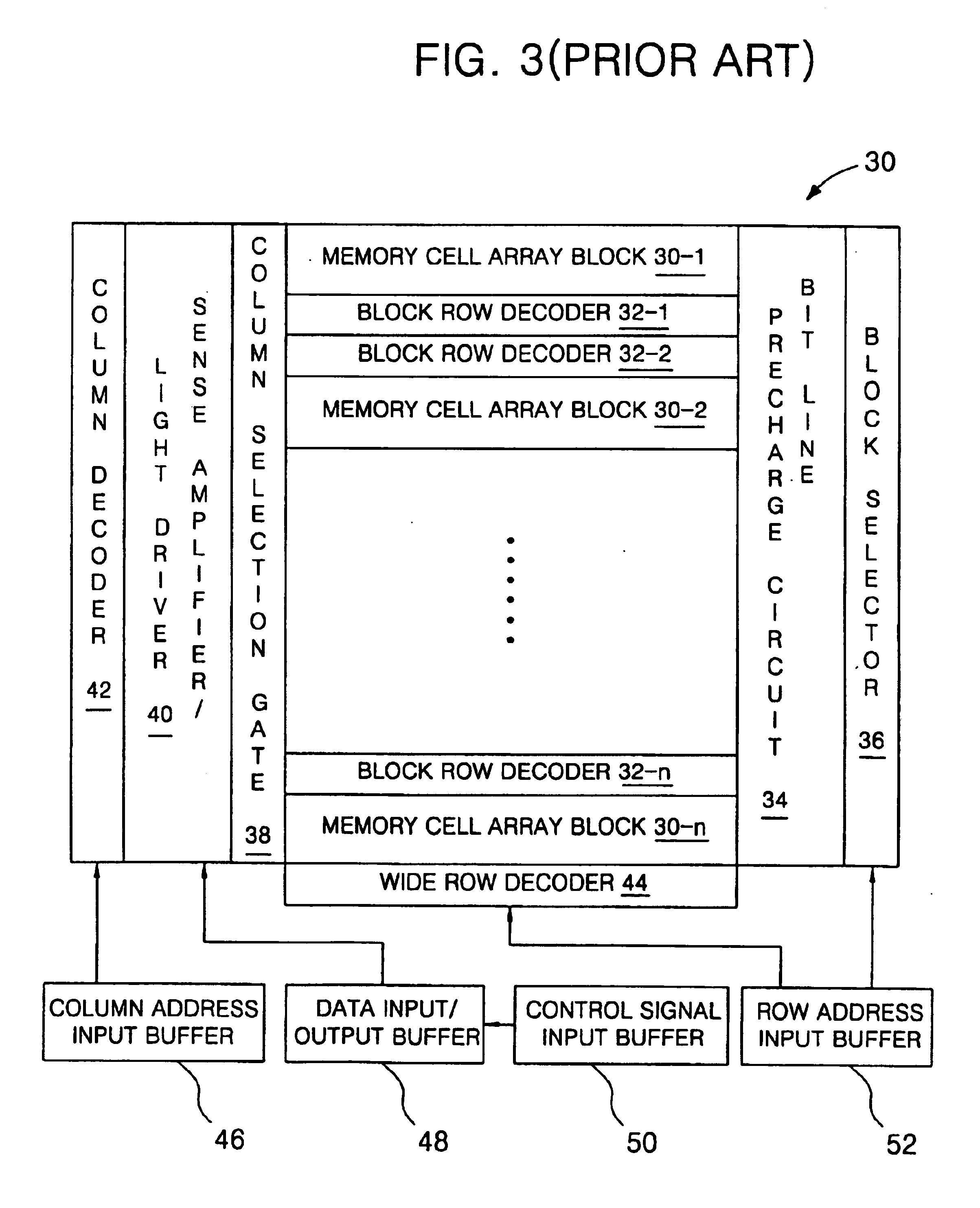
FIG. 3 is a block diagram illustrating the layout of an embodiment of a conventional semiconductor memory device, comprising memory cell array blocks 30-1, 30.2 . . . 30n, block row decoders 32-1, 32-2, . . . 32-n, a bit line pre charge circuit 34, a block selector 36, a column selection gate 38, a sense amplifier / light driver 40, a column decoder 42, a wide zone row decoder 44, a column address input buffer 46, a data input / output buffer 48, a control signal input buffer 50 and a row address input buffer 52.

The layout of the prior art semiconductor memory device includes the memory cell array 30 and neighboring circuits of controlling data input / output to the memory cell array 30.

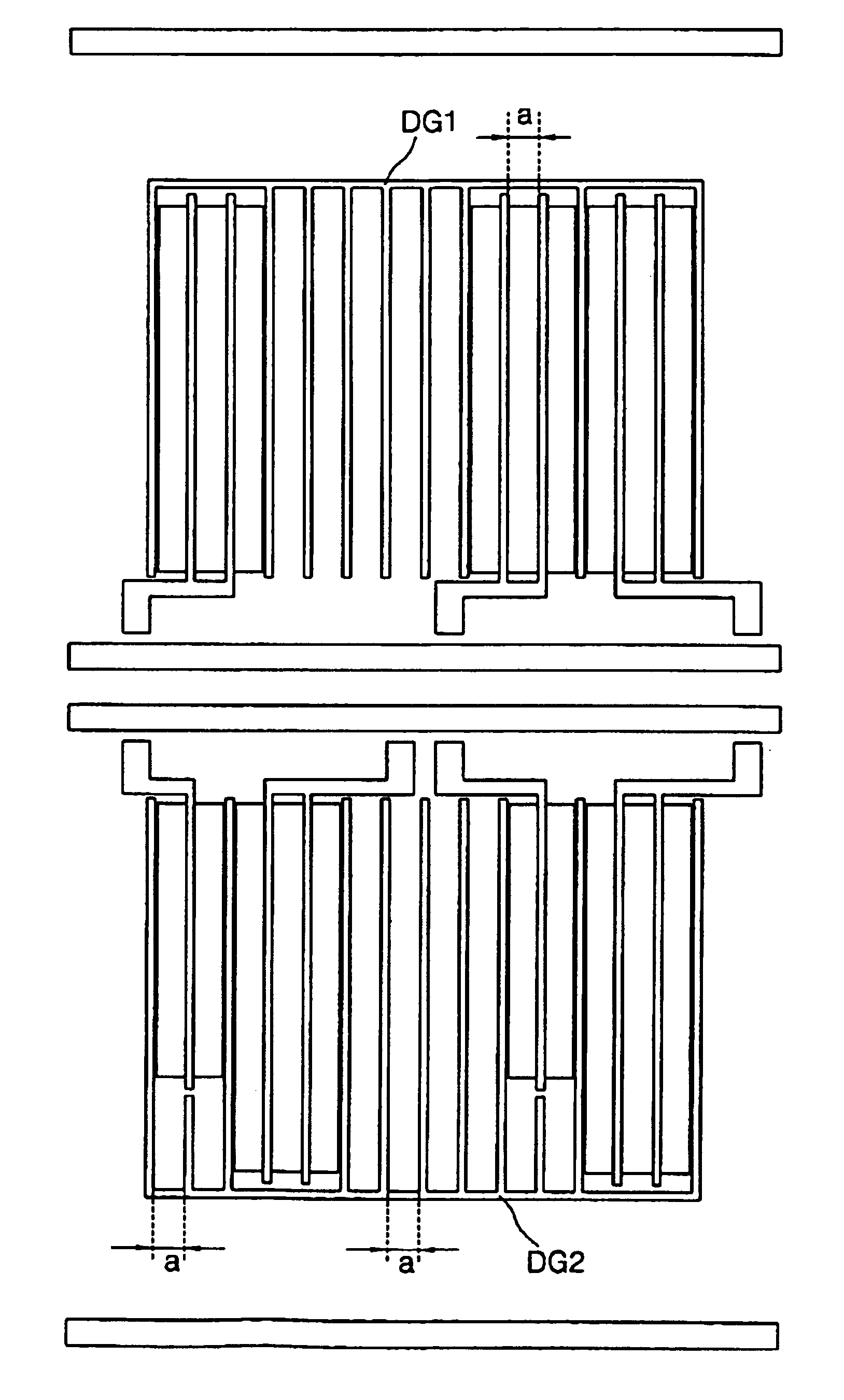
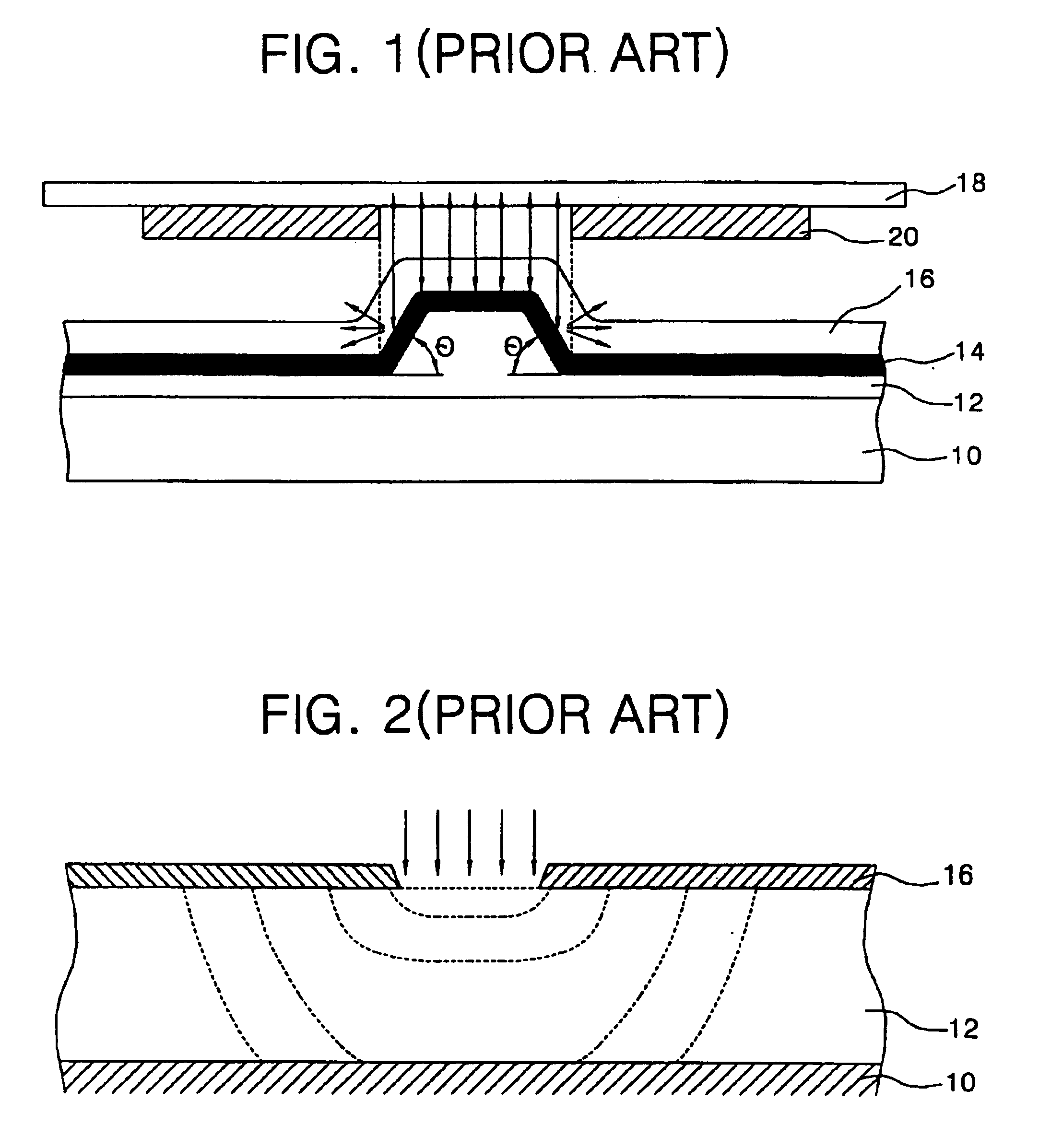
However, there is a problem in the conventional layout method of neighboring circuits of the semiconductor device in that the transistor gates of the neighboring circuits have been arranged at an irregular gap in the conventional layout method of the semiconductor device, thereby increasing variances in pr...


PUM


Abstract

A semiconductor device layout involving the following: arranging active regions of a plurality of transistors having at least more than one first and second electrodes disposed on a substrate; arranging a plurality of gates of transistors between more than one first and second electrodes of those active regions respectively by positioning at least more than one gates having predetermined width and length at a constant gap on the substrate; and arranging a plurality of dummy gates having predetermined width and length between a plurality of transistors (or between and outside transistors) at the same gap as that of the gates of transistors on the substrate, so that all the gates of transistors are arranged at a constant gap to minimize the variance of process deviations and accordingly reduce the difference of threshold voltage of transistors, thereby increasing reliability of the semiconductor device.

Description

FIELD OF THE INVENTIONThe present invention relates to a layout method of a semiconductor device, and more particularly to the layout method of the semiconductor device to reduce the variance in process deviations which may occur during photo and etching processes.BACKGROUND OF THE INVENTIONAs progress is made in functions of a system to which a semiconductor device is applied, functions of high speed and high integration in the semiconductor device have become important to the semiconductor device. Accordingly, the layout method is as important as the circuit design and fabricating in response to the trend of high speed and high integration of the semiconductor device.Some fabricating techniques for conventional semiconductor device, e.g., the uneven light reflection of the photo process and non-uniformity of the etching process, have brought about variances in process deviations at gates of transistors.The process deviation depends upon the extent of differences in the length of t...

Claims


Application Information

Patent Timeline
IPC IPC(8): H01L27/02H01L27/108H01L21/027H01L21/8242
CPCH01L27/0207H01L21/027
Inventor KANG, TAE-GYOUNG
Owner SAMSUNG ELECTRONICS CO LTD
Why Eureka
Try Eureka