
Phase change switches and circuits coupling to electromagnetic waves containing phase change switches

a phase change switch and circuit technology, applied in waveguide devices, bulk negative resistance effect devices, relays, etc., can solve the problems of difficult manufacturing and control, and conventional semiconductor switching devices typically will not operate to open and close circuits

Inactive Publication Date: 2005-06-07
LEIDOS
View PDF6 Cites 223 Cited by
  • Summary
  • Abstract
  • Description
  • Claims
  • Application Information

AI Technical Summary

Benefits of technology

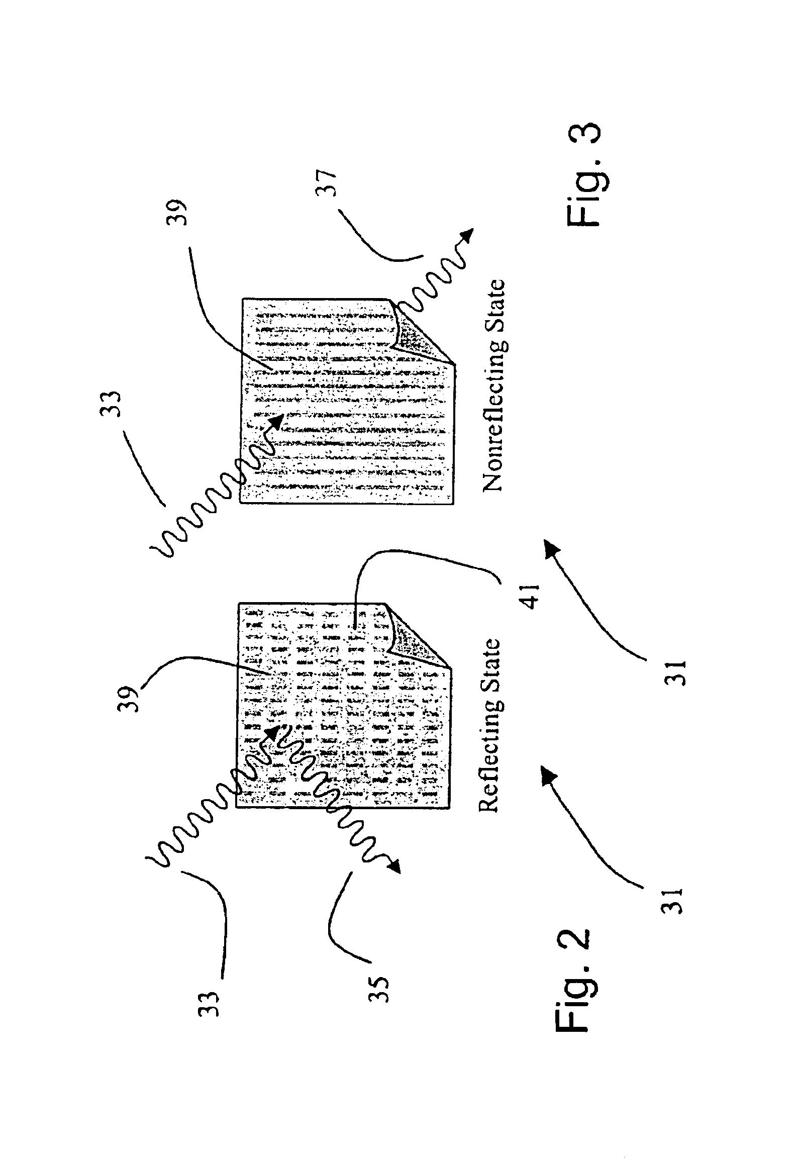
[0016]In another aspect, the first and second conductive elements in the grid forming the frequency selective surface are also made of the same compound as the switching material. In this aspect, the conductive elements and the connecting element may be switched together between low and high impedance states. More specifically, the circuit may be configured to cause only the connecting element to change its phase when an amount of energy is applied to the circuit. In this case, the first and second conductive elements, although made of the same compound, remain in the low impedance state.

Problems solved by technology

However, such applications involve complex structures that can be difficult to manufacture and control.
However, for the specific applications herein, conventional semiconductor switching devices typically will not operate to open and close circuits effectively to electromagnetic current flow in the frequency range of terahertz and above because at these frequencies, various intrinsic capacitances in the device structure can provide low impedance circuit paths that prevent the switch from operating as intended.

Method used


Image

  • Phase change switches and circuits coupling to electromagnetic waves containing phase change switches
  • Phase change switches and circuits coupling to electromagnetic waves containing phase change switches
  • Phase change switches and circuits coupling to electromagnetic waves containing phase change switches

Examples


Embodiment Construction

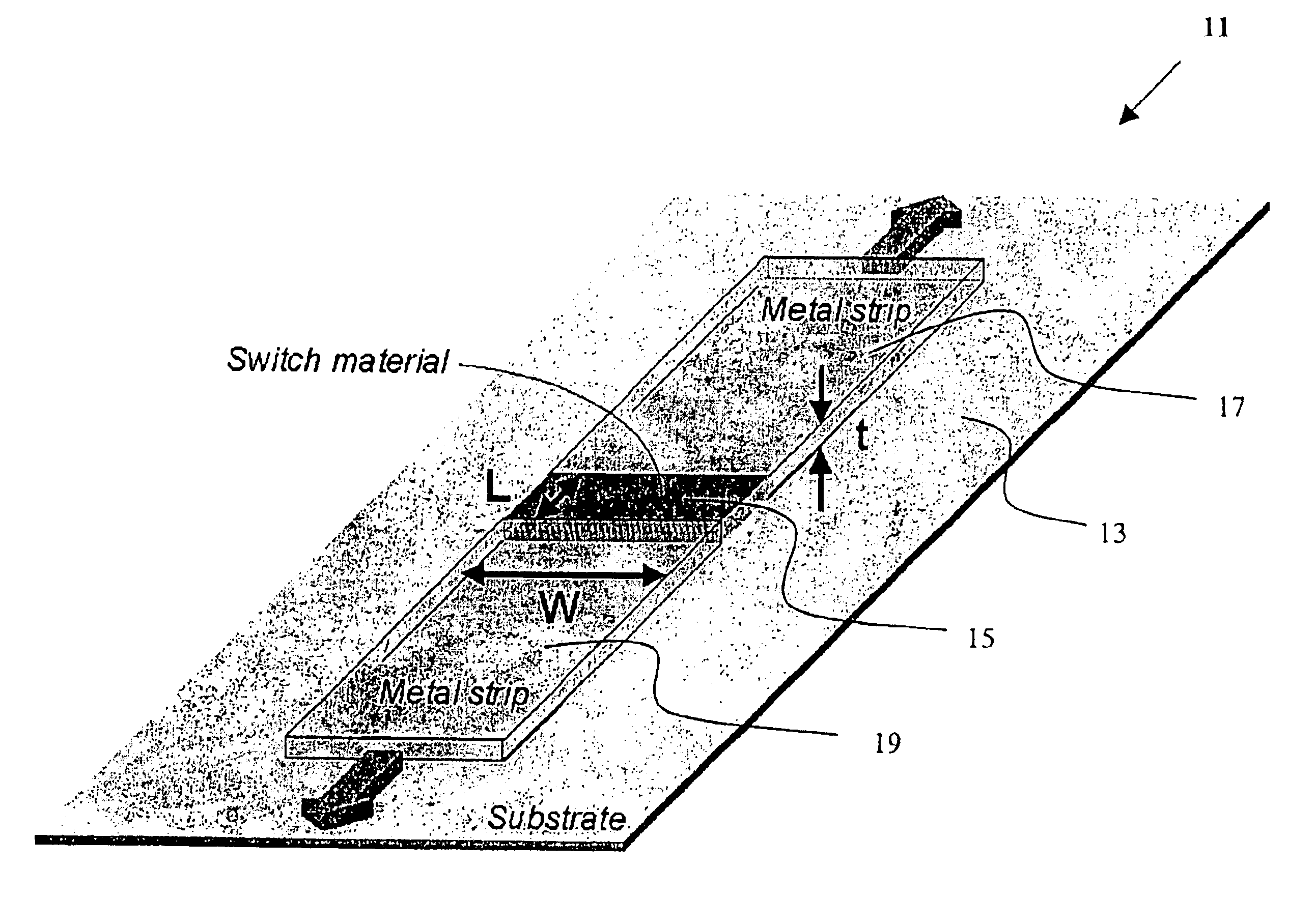
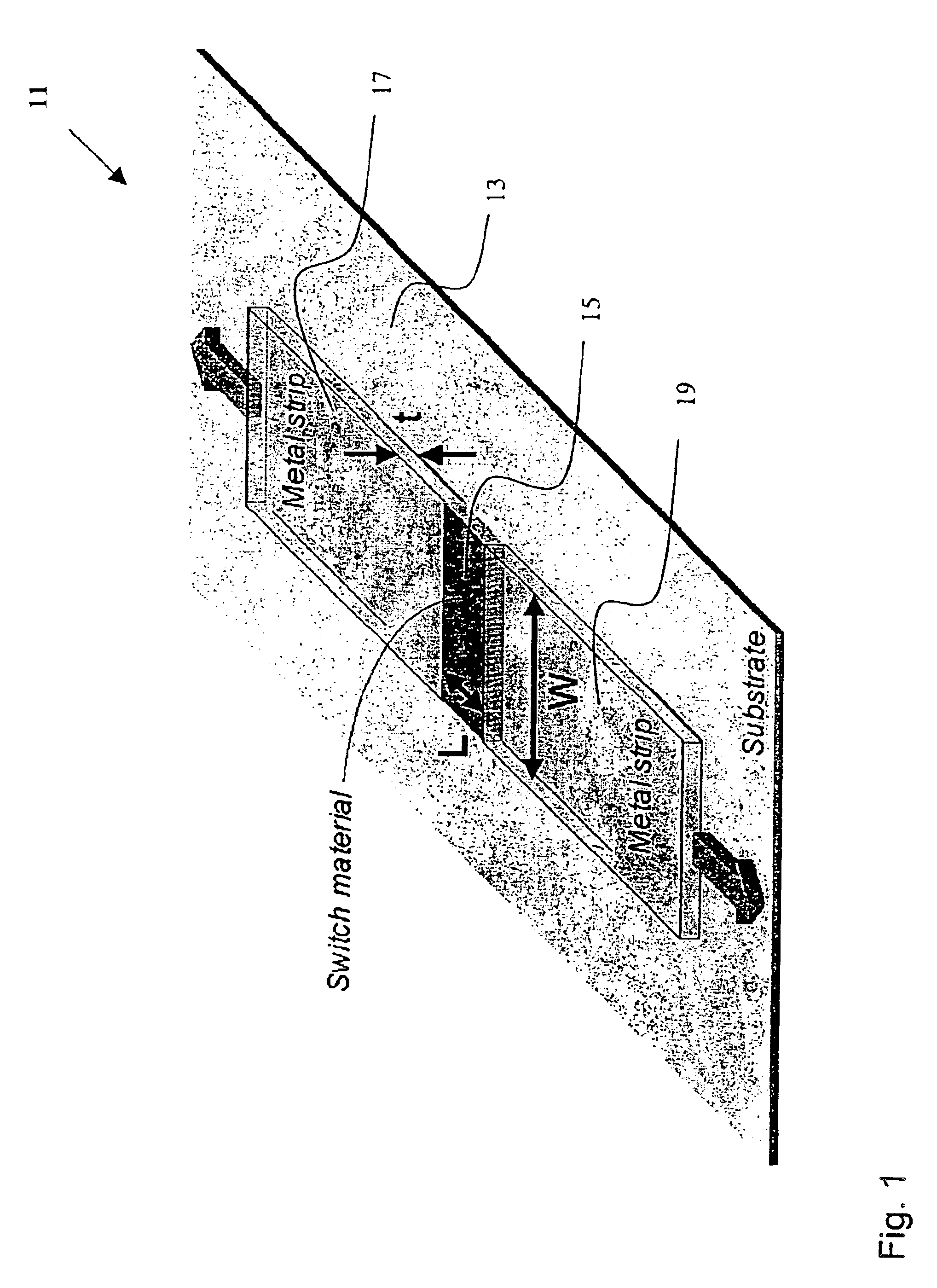
[0024]FIG. 1 schematically illustrates a switch 11 in accordance with the invention. The switch includes a substrate 13 having a switch material 15 deposited thereon to form a switch element, and connecting a first conductive element 17, typically a metal strip, to a second conductive element 19. The conductive elements 17 and 19 can be, for example, two circuit paths of an array or circuit such as a frequency selective surface array. The entire array can sit on top of a dielectric substrate 13, such as polyethylene.

[0025]The switch material 15 is typically a reversible phase change thin film material having a dynamic range of resistivity or impedance. An example of a typical switch material for use in accordance with the invention is a chalcogenide alloy, more specifically, Ge22Sb22Te56. Although a specific alloy has been described, it will be readily apparent to those of ordinary skill in the art that other equivalent alloys providing the same functionality may be employed Other s...


PUM


Abstract

A switch is used in circuits which interact with electromagnetic radiation. The switch includes a substrate for supporting components of the switch. A first conductive element on the substrate is provided for connecting to a first component of the circuit, and a second conductive element on the substrate serves to connect to a second component of the circuit. A switch element is made up of a switching material on the substrate and connects the first conductive element to the second conductive element. The switching material is a compound which exhibits a bi-stable phase behavior and is switchable between a first impedance state value and a second impedance state value upon the application of energy thereto. A circuit consisting of a plurality of conductive elements includes the switch for varying current flow which has been induced by the application of electromagnetic radiation.

Description

CROSS-REFERENCE TO RELATED APPLICATIONS[0001]This application is a divisional application of and claims priority to U.S. Utility patent application Ser. No. 09 / 851,619, filed May 9, 2001 now U.S. Pat. No. 6,730,928, entitled, “PHASE CHANGE SWITCHES AND CIRCUITS COUPLING TO ELECTROMAGNETIC WAVES CONTAINING PHASE CHANGE SWITCHES,” which is herein incorporated by reference in its entirety.BACKGROUND OF THE INVENTION[0002]1. Field of the Invention[0003]The invention relates to phase change switches, and more particularly, to phase change switches having a dynamic range of impedance. More specifically, the invention relates to such switches which can be employed in circuits such as on frequency selective surface arrays, for controlling current flow throughout the array, through the use of the switches. By controlling such current flow, the properties of the frequency selective surface array can be actively controlled.[0004]2. Background of the Invention[0005]A two-dimensional periodic ar...

Claims


Application Information

Patent Timeline
Patent Type & Authority Patents(United States)
IPC IPC(8): H01Q15/00H01P1/10
CPCH01Q15/002H01P1/10
Inventor WYETH, N. CONVERSGREEN, ALBERT M.
Owner LEIDOS
Learn More