

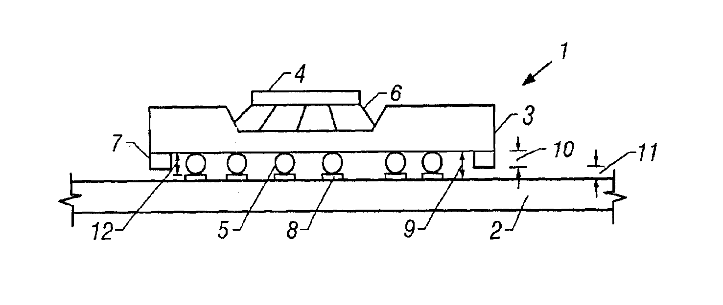
Attachment of surface mount devices to printed circuit boards using a thermoplastic adhesive
a technology of thermoplastic adhesive and printed circuit board, which is applied in the direction of dielectric characteristics, sustainable manufacturing/processing, and final product manufacturing, etc., can solve the problems of chip package/pcb solder joint failure, chip package/pcb solder joint adhesion becoming more problematic, and reducing the size of each solder ball and join
- Summary
- Abstract
- Description
- Claims
- Application Information
AI Technical Summary
Problems solved by technology
Method used
Image

Examples
working examples
[0182]Films of test adhesives were prepared by placing about 1 gram of adhesive pellets on a TEFLON™ plate resting on top of an aluminum plate preheated in an oven to a temperature of about 200° C. The pellets were allowed to heat for about 1 minute, after which a second TEFLON™ plate was laid on top of the molten pellets, followed by an aluminum plate weighted with a 5 lb copper bar. The assembly was allowed to heat for 10-15 minutes to about 200° C., removed from the oven, clamped into a vise, and squeezed to form a 7 mil thick film. For thicker films in the range of 10-15 mils, 2 grams of the adhesive pellets were placed on the TEFLON™ plates in the oven, and the assembly was pressed with appropriately sized shims. From the cooled sheets, the adhesive strips or squares were cut to size.[0183]FPE 1 is an acid functionalized polyethylene polymer functionalized with 10.5 wt % methacrylic acid having a melt index of 35.[0184]FPE 2 is an acid functionalized polyethylene polymer functi...
example 1
[0189]Thin strips measuring from 0.010″ to 0.015″ by ¼″ long were cut from the FPE 2 and the FPE 3 sheets. The FPE 2 strips were laid along the two parallel edges of a ¼″×¼″ glass slide 0.025″ thick, and also along two parallel edges on a BGA. With the polyolefin side up, the polyolefins were bonded to the glass slides and the BGA by heating to the first stage of a Thermal Cycle. The Thermal Cycle apparatus used was a ¼″ TEFLON™ board mounted on a lift under a Dayton IR lamp equipped with 900 watt lamps. Using temperature probe thermal waxes, the distance to the heat lamp to achieve a temperature of 180° C. was determined, and the time to reach 180° C. was determined to be 255 seconds. Once the test sample was exposed to the heat lamp for 255 seconds, the test sample was heated in a second stage by elevating the lift to a distance from the lamp predetermined to reach 260° C. within 45 seconds.
[0190]To bond the FPE 2 to the glass slide and the BGA, only the first stage thermal cycle ...
example 2
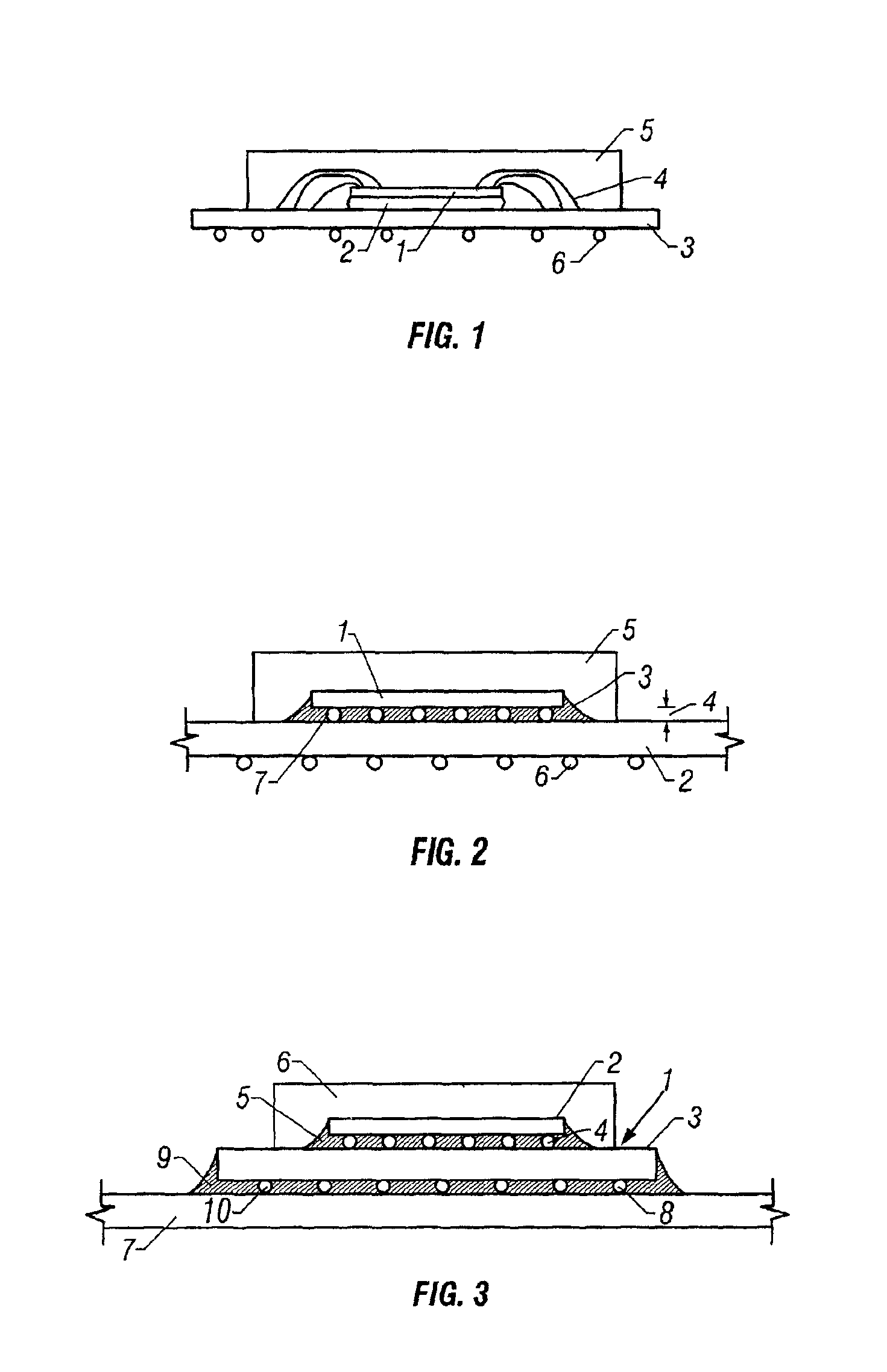
[0194]FPE 2 adhesive was cut into ¼″ strips having a thickness of about 0.024″, laid up along two parallel edges on a glass test slide measuring ¼″×¼″×0.040″, and heat bonded to the slide by subjecting the slide, adhesive side up, to a first stage in a Thermal Cycle (ambient to 180° C. over 255 seconds.). Once cooled, the glass slide was inverted, and mounted on top of a glass spacer sitting on the chip side of a printed circuit board wiped clean with acetone. The glass spacer was thick enough to provide a gap between the adhesive and the printed circuit board. The assembly was Thermally Cycled through both stages. Visual inspection revealed that the adhesive had sagged and flowed sufficiently to form a joint with the printed circuit board.
[0195]In the Mandrel bend test, the assembly passed through all deflections down to the 0.75″ mandrel.
PUM
| Property | Measurement | Unit |
|---|---|---|
| tensile strength | aaaaa | aaaaa |
| viscosity | aaaaa | aaaaa |
| viscosity | aaaaa | aaaaa |
Abstract
Description
Claims
Application Information