Silicon and silicon/germanium light-emitting device, methods and systems

a technology of light-emitting devices and silicon-germanium alloys, applied in the direction of instruments, optical elements, optical waveguide light guides, etc., can solve the problems of higher capacitance between wires, higher resistance in wires, and more electrical power

Inactive Publication Date: 2005-08-02
INTEL CORP
View PDF13 Cites 27 Cited by
  • Summary
  • Abstract
  • Description
  • Claims
  • Application Information

AI Technical Summary

Problems solved by technology

This results in a higher resistance in the wires and a higher capacitance between wires, which act to slow the electrical signal and requires more electrical power.
Such signal delays negatively impact the performance of IC chips and the computer as a whole.
This is because Si and Si / Ge, the materials presently used to form IC chips, have not been considered suitable for forming integral light sources because they have an indirect bandgap.
This makes for a relatively complicated and expensive on-chip or chip-to-chip optical communication system.
Further complicating chip-to-chip communications is the limited number of contact pads that can be fabricated onto a chip, as well as the limited available chip area.

Method used


Image

  • Silicon and silicon/germanium light-emitting device, methods and systems
  • Silicon and silicon/germanium light-emitting device, methods and systems
  • Silicon and silicon/germanium light-emitting device, methods and systems

Examples


Embodiment Construction

[0023]In the following detailed description of the embodiments of the invention, reference is made to the accompanying drawings that form a part hereof, and in which is shown by way of illustration specific embodiments in which the invention may be practiced. These embodiments are described in sufficient detail to enable those skilled in the art to practice the invention, and it is to be understood that other embodiments may be utilized and that changes may be made without departing from the scope of the present invention. The following detailed description is, therefore, not to be taken in a limiting sense, and the scope of the present invention is defined only by the appended claims.

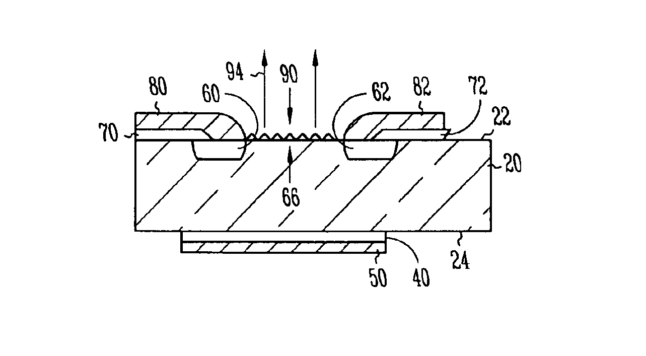
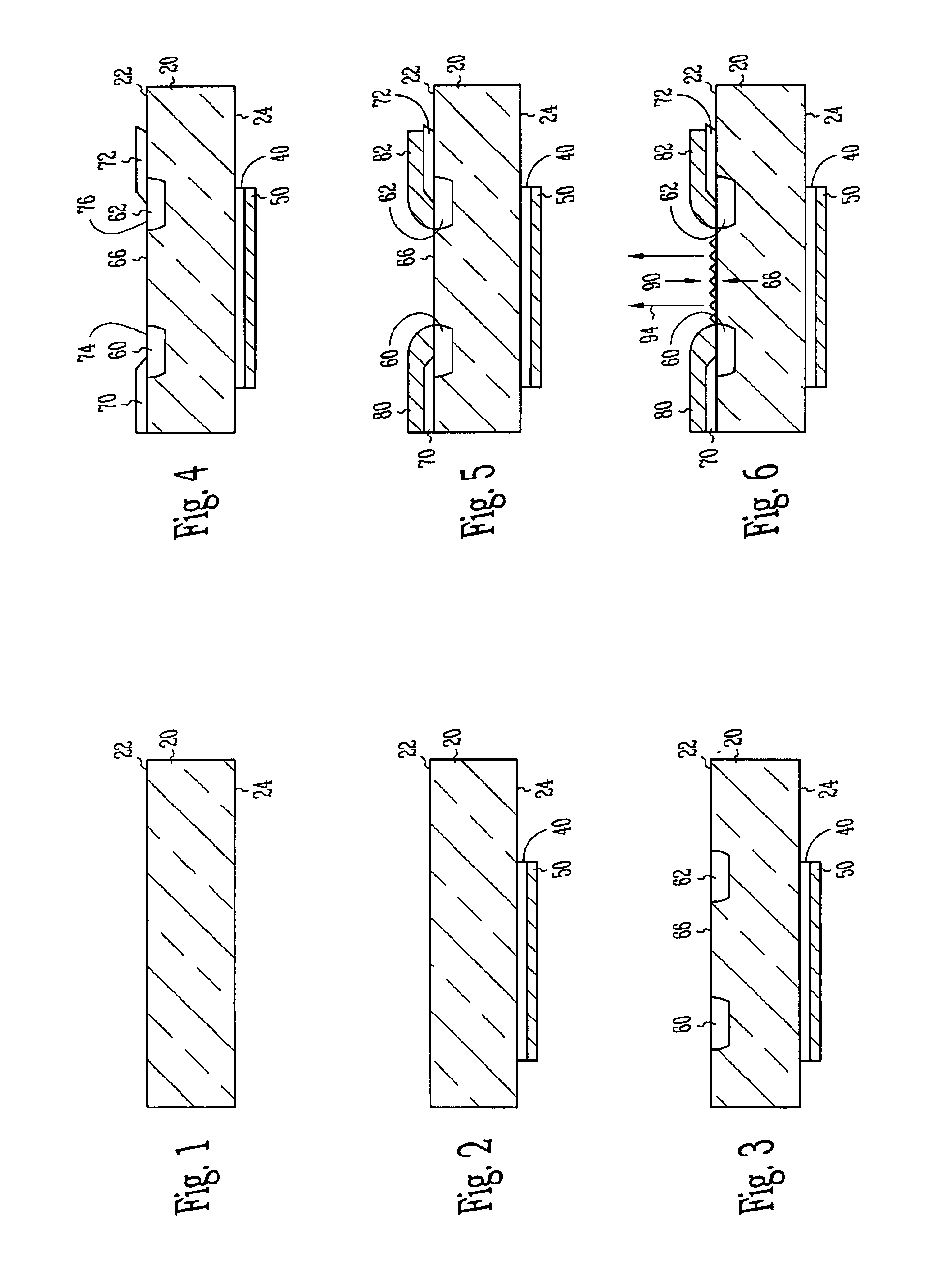
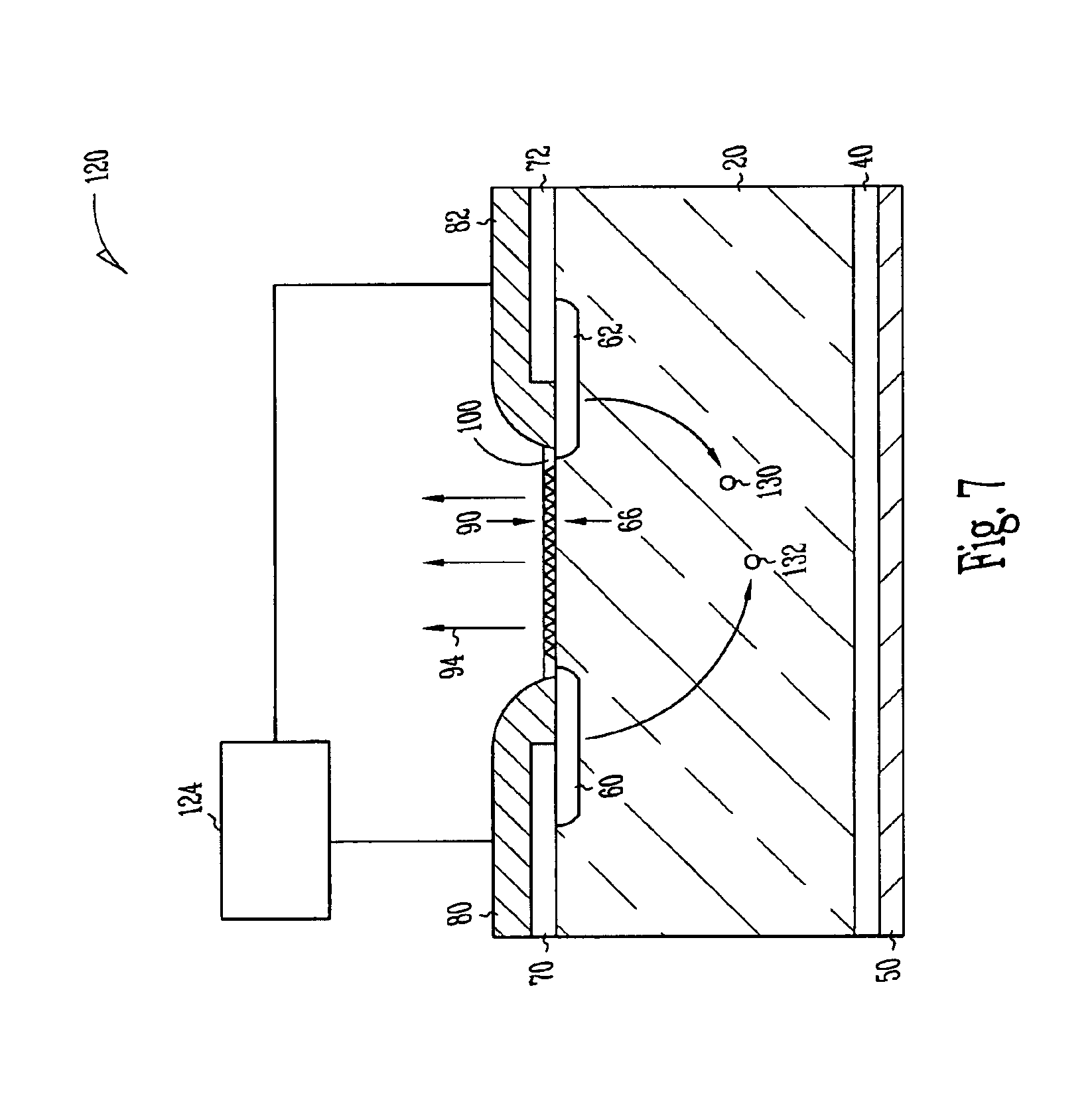
[0024]With reference to FIGS. 1-7 described briefly above, a method of forming an example embodiment of the light-emitting device of the present invention is now described.

[0025]In FIG. 1, a substrate 20 with an upper surface 22 and a lower surface 24 is provided. In one embodiment, the substrate is fl...


PUM


Abstract

A light-emitting device and optical communication system based on the light-emitting device is disclosed. The light-emitting device is formed in a float-zone substrate. The light-emitting device includes on the substrate lower surface a reflective layer and on the upper surface spaced apart doped regions. The portion of the upper surface between the doped regions is textured and optionally covered with an antireflection coating to enhance light emission. The light-emitting device can operate as a laser or as a light-emitting diode, depending on the reflectivities of the antireflection coating and the reflective layer.

Description

TECHNICAL FIELD[0001]The present invention relates to light-emitting devices formed in Si or Si / Ge and to optical communications systems employing same.BACKGROUND INFORMATION[0002]Modern computers are formed from a variety of different types of integrated circuit (IC) chips, such as controllers, central processing units (CPUs) and memory. On-chip and chip-to-chip interconnections within a computer are typically made with metal wires. As ICs become more integrated, the wires becomes narrower and more closely spaced. This results in a higher resistance in the wires and a higher capacitance between wires, which act to slow the electrical signal and requires more electrical power. The degree to which the electrical signal is slowed is also proportional to the square of the length of the wire. Such signal delays negatively impact the performance of IC chips and the computer as a whole.[0003]To solve this problem, in-chip and chip-to-chip optical interconnections using light sources and w...

Claims


Application Information

Patent Timeline
Patent Type & Authority Patents(United States)
IPC IPC(8): G02B6/13G02B6/12G02B6/122G02B6/42G02B6/43G02B6/138H01L33/00H01L31/173H01L31/16H01L33/34
CPCG02B6/12004G02B6/1221G02B6/13G02B6/138G02B6/42H01L33/34G02B6/4228G02B6/43H01L31/173G02B2006/12121G02B6/4214
Inventor GARDNER, DONALD S.KARNIK, TANAYXU, JIANPINGBORKAR, SHEKHAR Y.
Owner INTEL CORP
Why Eureka
Try Eureka