Semiconductor device realizing characteristics like a SOI MOSFET

a technology of soi mosfet and semiconductor device, which is applied in the direction of semiconductor device, electrical apparatus, transistor, etc., can solve the problems of increasing performance degradation, unwanted increase of parasitic resistance value, and relatively less quality of soi substra

Inactive Publication Date: 2005-08-16
KIOXIA CORP
View PDF14 Cites 20 Cited by
  • Summary
  • Abstract
  • Description
  • Claims
  • Application Information

AI Technical Summary

Problems solved by technology

Unfortunately in view of the quest for higher integration and miniaturization, the advantage of FD-SOIFETs does not come without accompanying several penalties.
Second, the use of such ultrathin silicon layers would result in an unwanted increase in parasitic resistance values.
Third, as a channel region surrounded by oxide films which are ordinarily less in thermal conductivity than silicon, the conductivity of heat generated in self-heatup regions near a drain is made inferior, resulting in an increase in degradation of performance.
Another penalty is a problem that the SOI substrates are relatively less in quality whereas gate dielectric films stay less in reliability, causing possible plasma damages to increase accordingly.
A further penalty lies in high price of the SOI substrates at least at the present time.
The proposed pseudo-SOIFET structures are still encountered with many problems to be solved, one of which is the difficulty in obtaining any sufficient performance on the order of submicrons of minimum feature size.
This is a serious bar to suppression of short-channel effects in the case of further miniaturization or shrinkage.
Additionally if a semiconductor layer of such channel region is formed of an impurity-doped layer low in impurity concentration enough to realize a fully depleted element, then punch-through can disadvantageously take place in cases where the gate length (channel length) is shortened to be on the order of submicrons.
This would result in an undesired increase in junction capacitance of the source / drain, thereby making difficult achievement of high-speed operabilities.
Simple use of such ion implantation methods for obtaining the p / n− / p channel structure can reach a limit in further reduction of channel region impurity concentration and thickness.

Method used


Image

  • Semiconductor device realizing characteristics like a SOI MOSFET
  • Semiconductor device realizing characteristics like a SOI MOSFET
  • Semiconductor device realizing characteristics like a SOI MOSFET

Examples


first embodiment

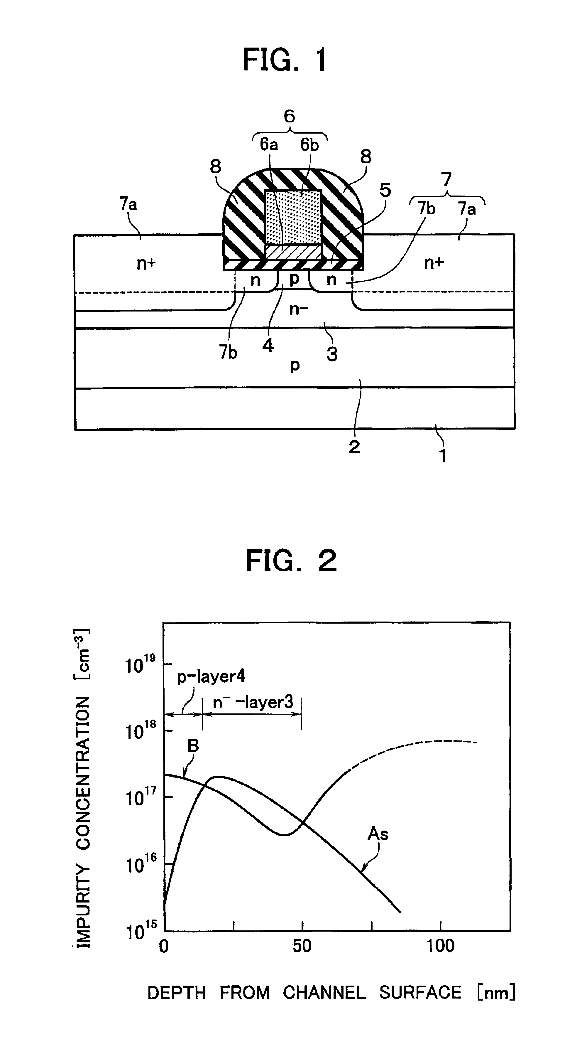
[0041]Referring to FIG. 1, there is illustrated a sectional view of a structure of main part of a MISFET in accordance with a first embodiment of the invention.

[0042]A silicon substrate 1 has its top surface in which a p-type impurity doped layer 2 is formed by well ion implantation techniques. Formed on this p-type layer 2 are a lightly-doped n (n−) type impurity doped layer of low impurity concentration and further a p-type impurity doped layer 4 for use as a channel region. These layers 2-4 make up a multilayer lamination structure with p / n− / p junction. Certain portions of this p / n− / p junction multilayer structure—at least the upper p-type layer 4 and its underlying n−-type layer 3—are fabricated by epitaxial growth process and ion implantation process in combination, as will be described in detail later in the description.

[0043]As shown in FIG. 1, a gate electrode 6 is formed over the p-type layer 4 for use as the channel region, with a gate dielectric film 5 being interposed th...

second embodiment

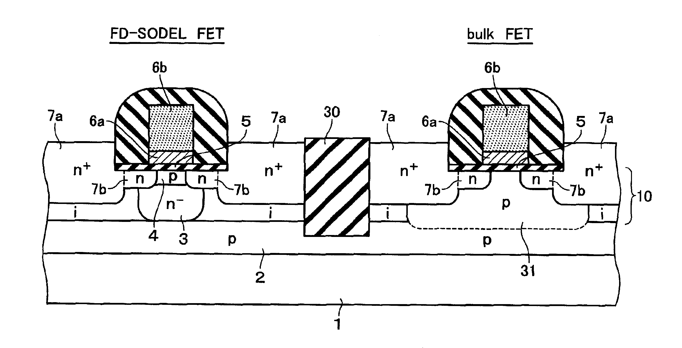
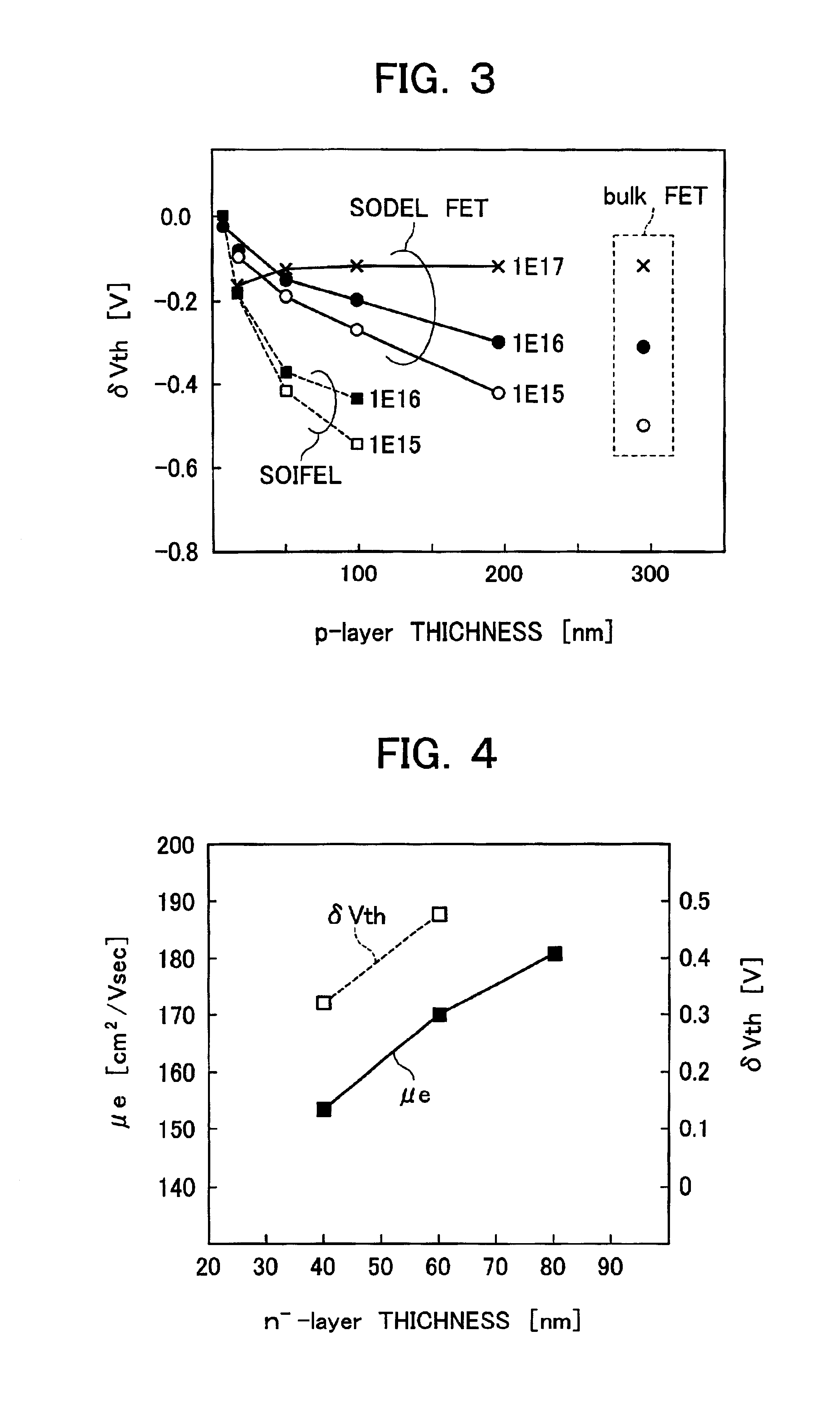
[0073]In the first embodiment above, even with optimization of the impurity concentration and thickness values of the p / n− / p junction multilayer structure, punch-through phenomena will possibly become hardly negligible between the source and drain in highly integrated semiconductor devices of the generation with 50-nm gate lengths or later generations.

[0074]See FIG. 14. This diagram depicts a sectional view of an SODELFET structure capable of preventing any punch-through with increased reliability in accordance with a second embodiment of the invention, wherein the depiction here is shown in a way corresponding to FIG. 1. This embodiment is similar to that of FIG. 1 except that p-type layers 9 are additionally provided as “halo” regions. These layers are buried in the n−-type layer 3 at locations immediately beneath the source / drain extension regions 7b, respectively. As in the first embodiment, appropriate value setting of the impurity concentration and thickness of p-type layer 4 ...

third embodiment

[0078]Turning to FIG. 15, there is shown in a manner corresponding to FIG. 1 a sectional view of an SODELFET also embodying the invention, which employs selective ion implantation to selectively fabricate the intended p / n− / p junction multilayer structure in a specified region immediately beneath a gate electrode. Unlike the embodiment of FIG. 1, arsenic (As) ion implantation is selectively done only at a channel body forming portion of an undoped or “nondoped” epitaxially grown silicon layer 10, thereby forming an n−-type layer 3. Thus the resulting extension regions 7b of source / drain diffusion layers 7 are such that the bottom surface of each is in contact with its underlying n−-type layer 3 while a respective n+-type low-resistivity region 7a has its bottom face residing within the nondoped silicon layer 10.

[0079]As per the p-type layer 4 for use as a transistor channel region also, this is manufacturable similarly by selective ion implantation of boron (B).

[0080]Forming the n−-t...


PUM


Abstract

In a semiconductor device, source / drain layers have a low resistivity region and an extension region extending from the low resistivity region toward the channel region. The extension regions are lower in impurity concentration and shallower in depth than the low resistivity regions. The device also has a first impurity-doped layer formed in the channel region between the source / drain layers, a second impurity-doped layer formed under the first impurity-doped layer, and a third impurity-doped layer formed under the second impurity-doped layer. The first impurity-doped layer is equal or less injunction depth than the extension regions. The second impurity doped layer has impurity concentration and thickness to be fully depleted due to a built-in potential as created between the first and third impurity-doped layers.

Description

CROSS-REFERENCE TO RELATED APPLICATIONS[0001]This application is based on and claims the benefit of priority from prior Japanese Patent Application No. 2001-010449, filed on Jan. 18, 2001, the entire contents of which are incorporated herein by reference.BACKGROUND OF THE INVENTION[0002]1. Field of the Invention[0003]This invention relates generally to semiconductor devices using bulk semiconductor for achievement of highly miniaturized transistors with enhanced performance. The invention also relates to a method of fabricating the same.[0004]2. Description of Related Art[0005]Today, metal insulator semiconductor field effect transistors (MISFETs) using silicon-on-insulator (SOI) substrates with a fully depleted channel region are under diligent research and development at some leading companies and laboratories, for use as transistors suitable for microfabrication and performance enhancement schemes. The MOSFETs of this type will be referred to as fully depleted SOIFETs or simply F...

Claims


Application Information

Patent Timeline
Patent Type & Authority Patents(United States)
IPC IPC(8): H01L21/02H01L21/70H01L21/336H01L29/78H01L29/10H01L29/02H01L21/8234H01L21/8238H01L27/085H01L27/088H01L29/66H01L29/49H01L29/40
CPCH01L21/823412H01L21/823807H01L27/0883H01L29/1083H01L29/66628H01L29/7834H01L29/4958H01L29/78
Inventor INABA, SATOSHI
Owner KIOXIA CORP
Why Eureka
Try Eureka