Semiconductor memory device with reduced chip area and improved redundancy efficency

Inactive Publication Date: 2005-09-13
SAMSUNG ELECTRONICS CO LTD
View PDF2 Cites 1 Cited by
  • Summary
  • Abstract
  • Description
  • Claims
  • Application Information

AI Technical Summary

Benefits of technology

[0010]Accordingly, the present invention is directed to a semiconductor memory device that obviates one or more problems due to limitations and disadvantages of the related art. Embodiments of the invention provide a semiconductor memory device having a redundancy circuit that minimizes the circuit area while improving the redundancy efficiency.

Problems solved by technology

This increase in the size of the memory chip results in a lower wafer yield.
However, in the case where only the defective memory cells or the defective bit lines should be repaired, the sector address fuses of the redundancy circuit are not used.
This implies that the redundancy efficiency is low with respect to the area of the redundancy circuit.

Method used


Image

  • Semiconductor memory device with reduced chip area and improved redundancy efficency
  • Semiconductor memory device with reduced chip area and improved redundancy efficency
  • Semiconductor memory device with reduced chip area and improved redundancy efficency

Examples


Embodiment Construction

[0018]Reference will now be made in detail to preferred embodiments of the invention, examples of which are illustrated in the accompanying drawings. Specifically, a nonvolatile memory device having EPROM memory cells will be disclosed. However, the invention is not limited to nonvolatile memory devices having EPROM memory cells.

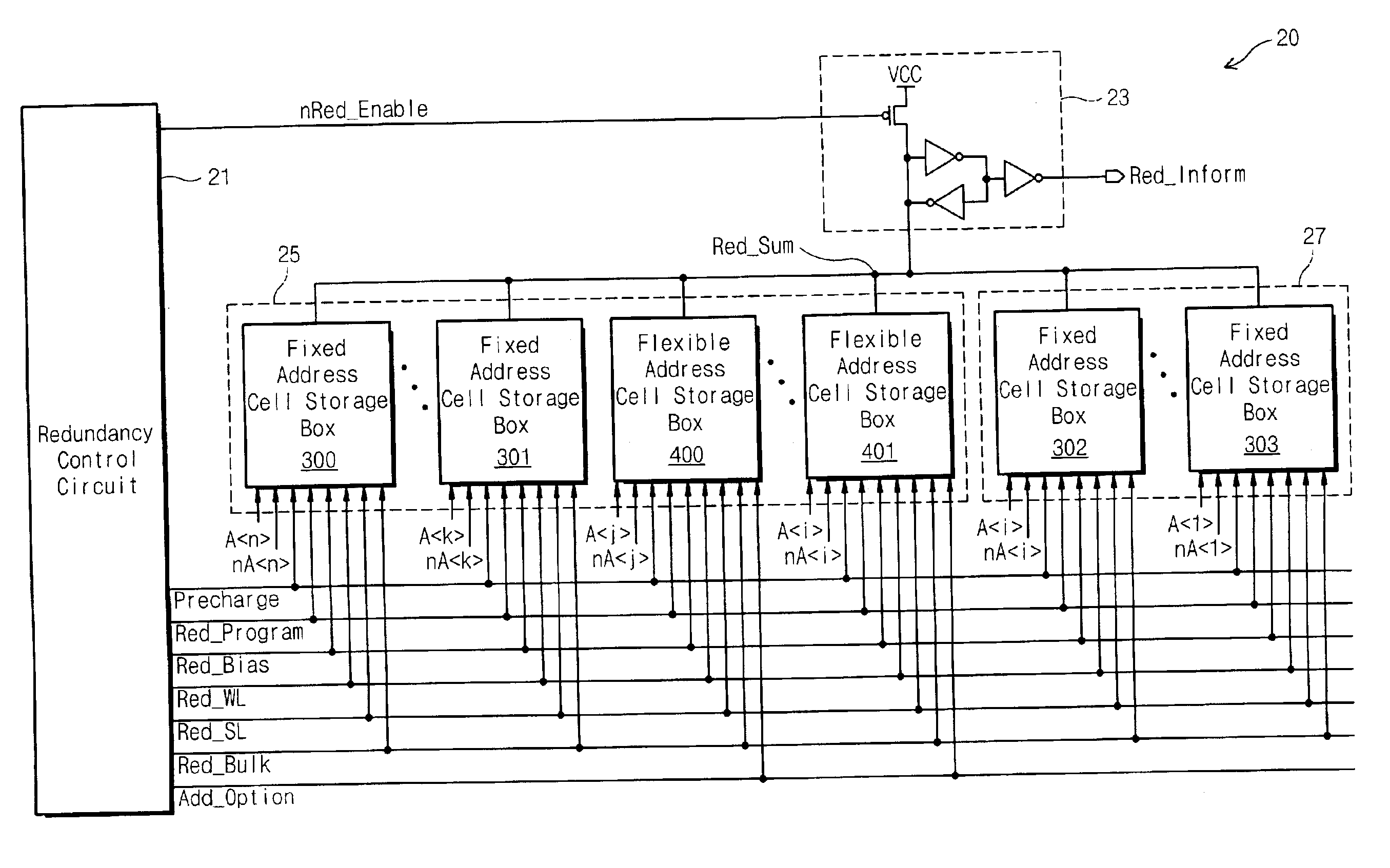
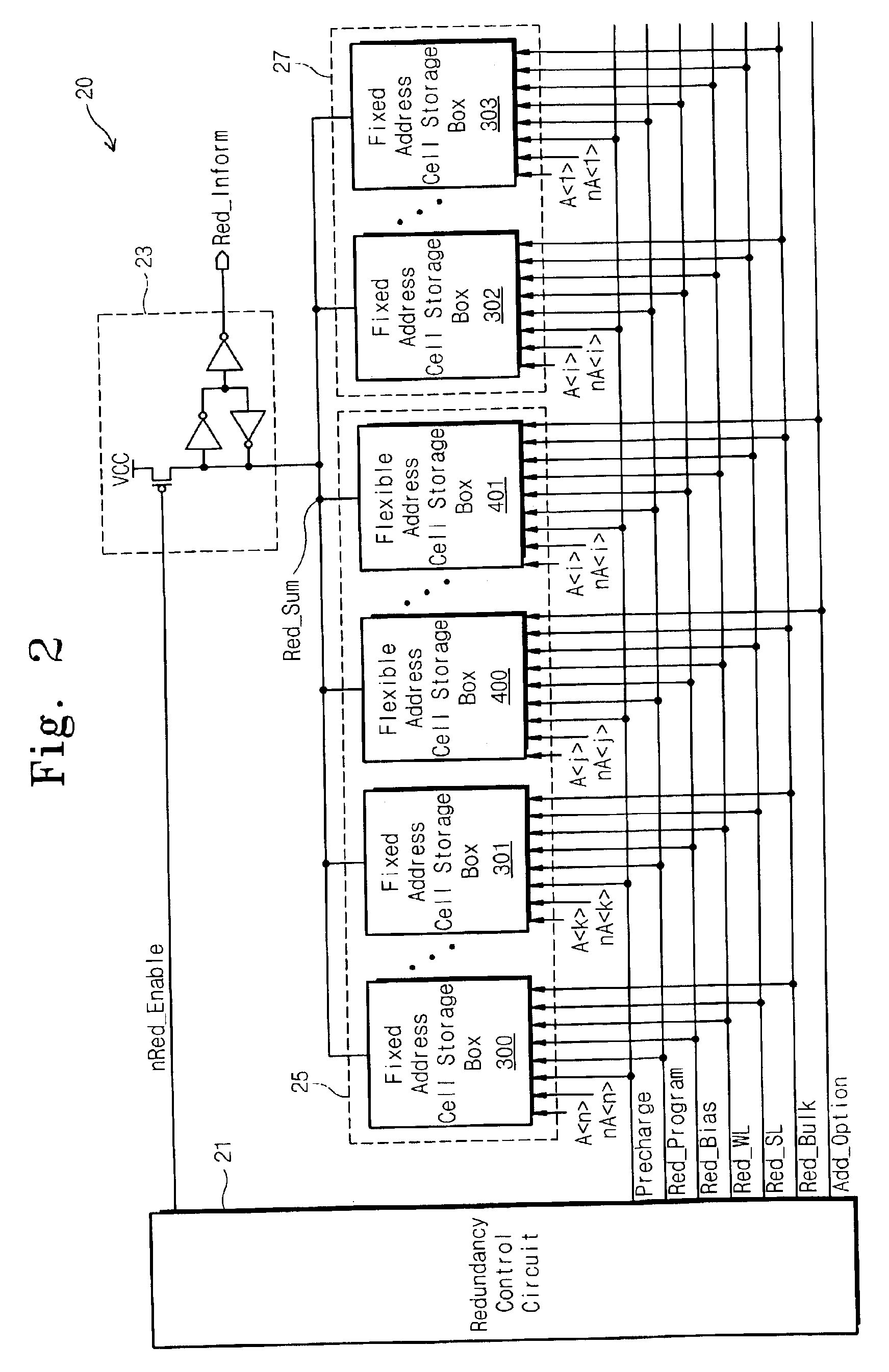
[0019]A redundancy circuit according to an embodiment of the invention is illustrated in FIG. 2. Referring to FIG. 2, a redundancy circuit 20 includes a redundancy control circuit 21, a redundancy signal generator 23, a sector selector 25 and a bit line selector 27. The redundancy control circuit 21 generates a redundancy enable signal nRed_Enable, a precharge signal Precharge, a redundancy program signal Red_Program, a redundancy bias signal Red_Bias, a redundancy word line signal Red_WL, a redundancy source signal Red_SL, a redundancy bulk signal Red_Bulk, and a redundancy option signal Add_Option.

[0020]FIG. 3 illustrates the fixed address cell storage box...


PUM


Abstract

A redundancy circuit embedded in the semiconductor memory device includes a sector selector and a bit line selector. The bit line selector repairs defective bit lines and the sector selector repairs defective global bit lines and selectively repairs defective bit lines. The sector selector includes a fixed address cell storage box for storing addresses of the defective bit lines and a flexible address cell storage box for storing addresses of the defective global bit lines. The circuit area is minimized since the coding unit corresponding to a sector address is not included in the bit line selector. The repair rate of defective bit lines is improved since the sector selector operates selectively as the bit line selector.

Description

CROSS REFERENCE TO RELATED APPLICATIONS[0001]This application claims priority to Korean Patent Application 2002-23656, filed on Apr. 30, 2002, the contents of which are hereby incorporated by reference in their entirety.BACKGROUND OF THE INVENTION[0002]1. Field of the Invention[0003]The present invention relates to a semiconductor memory device, and more particularly, to a semiconductor memory device having a redundancy circuit to reduce the chip area and to improve the redundancy efficiency.[0004]2. Description of the Related Art[0005]As the goals of achieving higher integration and larger capacity for semiconductor memory devices are reached, the size of a memory chip becomes increasingly larger. This increase in the size of the memory chip results in a lower wafer yield. Redundancy technology to repair defective memory cells has been used in semiconductor memory devices as one of the ways to increase the wafer yield. Redundancy technology provides a semiconductor memory device wi...

Claims


Application Information

Patent Timeline
IPC IPC(8): G11C29/00G11C16/04G11C16/06G11C29/04
CPCG11C29/789G11C29/808G11C16/0441G11C29/00
Inventor LEE, BYEONG-HOONLEE, SEUNG-KEUN
Owner SAMSUNG ELECTRONICS CO LTD
Why Eureka
Try Eureka