Pitcher-shaped active area for field effect transistor and method of forming same

a field effect transistor and active area technology, applied in the field of semiconductor devices, can solve problems such as low electric field, and achieve the effects of reducing contact resistance, increasing transistor on-current, and reducing transistor serial resistan

Inactive Publication Date: 2005-11-01
INFINEON TECH AG
View PDF14 Cites 9 Cited by
  • Summary
  • Abstract
  • Description
  • Claims
  • Application Information

AI Technical Summary

Benefits of technology

The present invention provides an improved design for a field effect transistor (FET) that increases the amount of current it can handle, reduces resistance, and simplifies the process of connecting to other components in an integrated circuit. This is achieved by widening the top parts of the active area without changing the length of the gate. This design helps maintain the benefits of a wider active area while also increasing the on-current of the transistor.

Problems solved by technology

The technical problem addressed in this patent text relates to improving the efficiency and functionality of semiconductor devices, particularly field effect transistors (FETs), through the development of an enhanced active area structure that can increase transistor on-current while minimizing serial resistance and contact resistance. This will require overcoming limitations related to conventionally patterned openings for the active areas of FETs, including restricted access due to small ground rules and uneven electrostatic fields resulting in lower thresholds at the edges of the active area.

Method used


Image

  • Pitcher-shaped active area for field effect transistor and method of forming same
  • Pitcher-shaped active area for field effect transistor and method of forming same
  • Pitcher-shaped active area for field effect transistor and method of forming same

Examples


Embodiment Construction

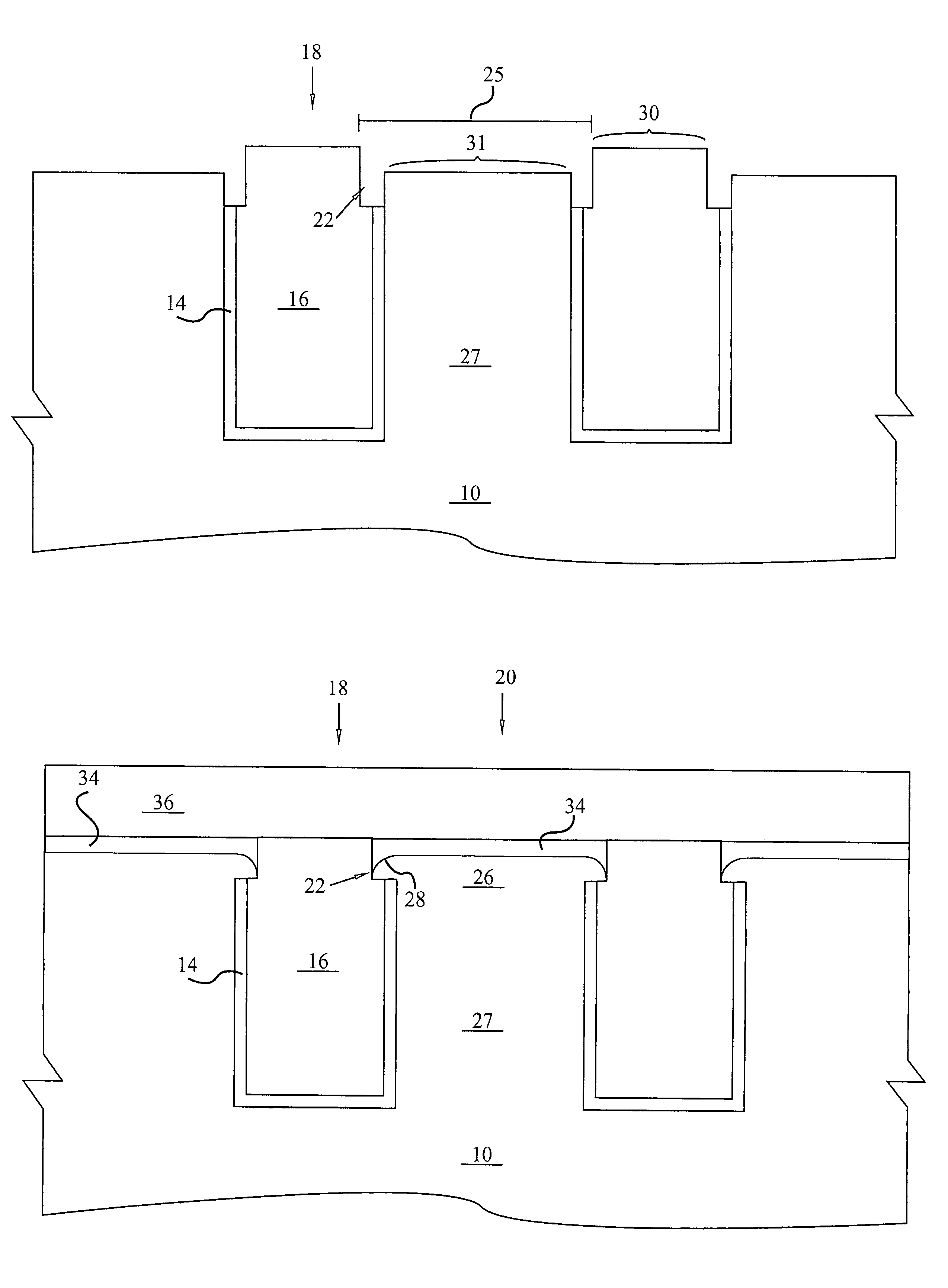
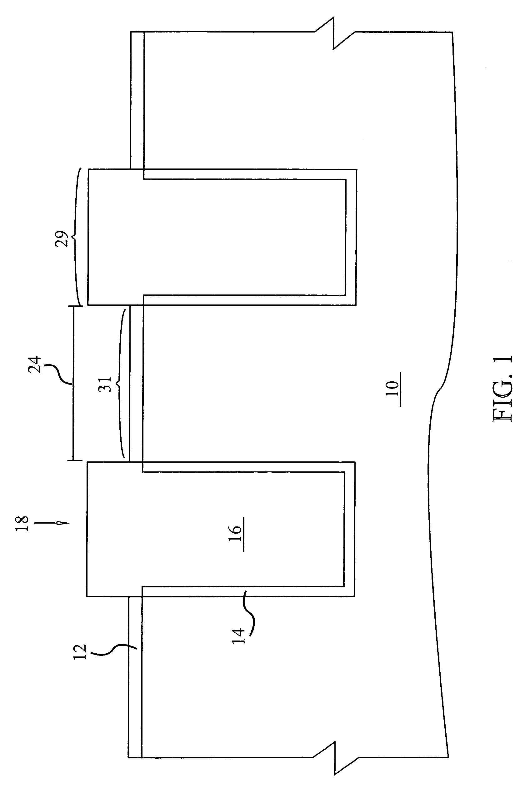
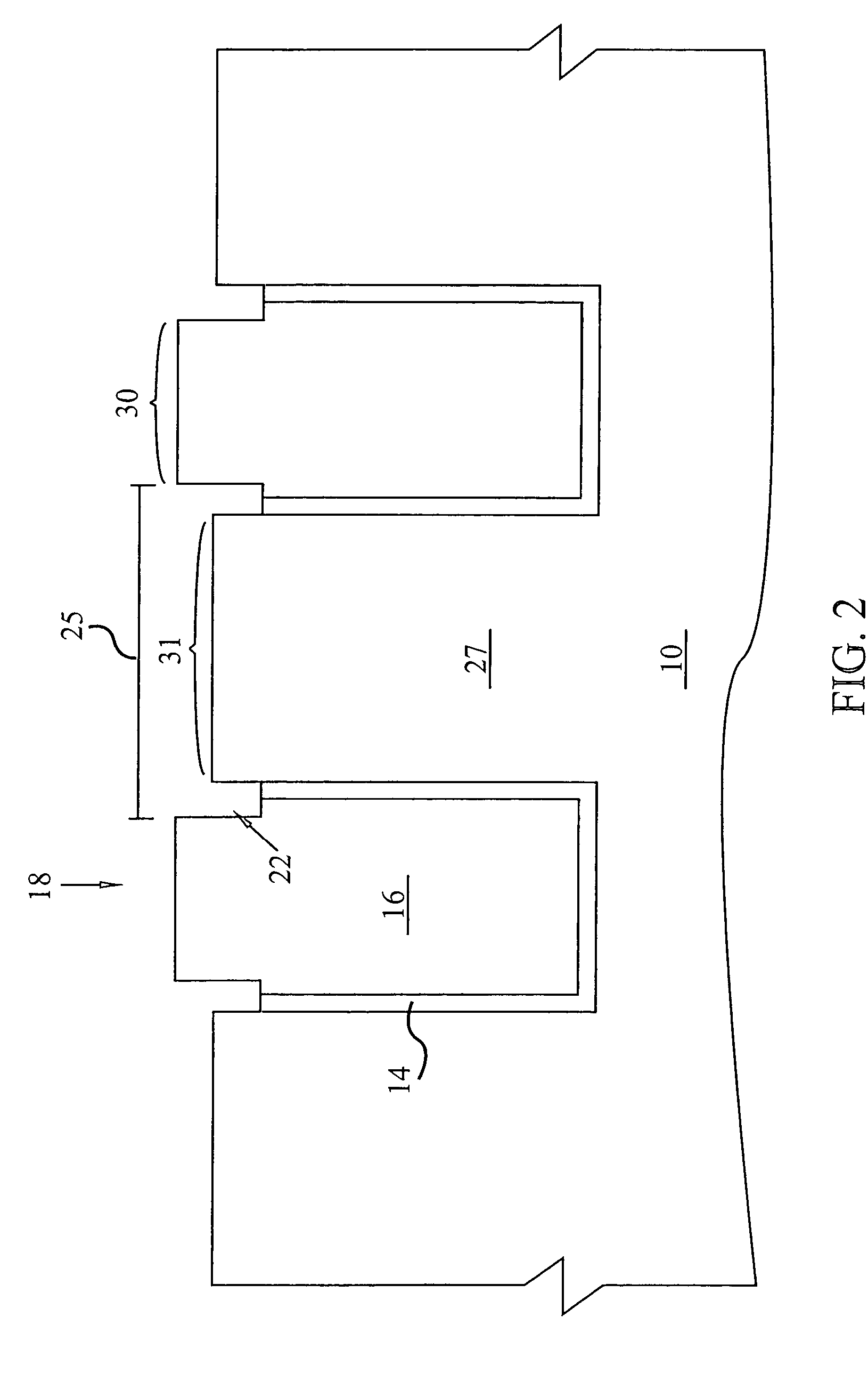
[0017]Although the present invention may be readily adapted to a variety of methods of fabricating a FET, with reference to FIGS. 1–4, the following is an example of a method of fabrication. FIGS. 1–4 are cross-sectional views depicting various stages during the fabrication process of pitcher-shaped active area 20 of a FET, as depicted in FIGS. 3 and 4. Generally, the improved fabrication method of present invention may form pitcher-shaped active area 20 by implementing a step to form divots 22 in top portions of the side walls of STI structures 18. Following the formation of divots 22, a step may be implemented to migrate substrate material into STI divots 22, thereby forming widened top portion 26 of pitcher-shaped active area structure 20. It will be understood by one of ordinary skill in the art that the invention is not limited to the specific structures illustrated in the drawings or to the specific steps detailed herein. It will also be understood that the invention is not li...


PUM


Abstract

An improved pitcher-shaped active area for a field effect transistor that, for a given gate length, achieves an increase in transistor on-current, a decrease in transistor serial resistance, and a decrease in contact resistance. The pitcher-shaped active area structure includes at least two shallow trench insulator (STI) structures formed into a substrate that defines an active area structure, which includes a widened top portion with a larger width than a bottom portion. An improved fabrication method for forming the improved pitcher-shaped active area is also described that implements a step to form STI structure divots followed by a step to migrate substrate material into at least portions of the divots, thereby forming a widened top portion of the active area structure. The fabrication method of present invention forms the pitcher-shaped active area without the use of lithography, and therefore, is not limited by the smallest ground rules of lithography tooling.

Description


Claims


Application Information

Patent Timeline
Owner INFINEON TECH AG
Why Eureka
Try Eureka