Alignment of MTJ stack to conductive lines in the absence of topography

a technology of conductive lines and mtj stacks, applied in the direction of semiconductor devices, semiconductor/solid-state device details, electrical devices, etc., can solve problems such as process disconnection, and achieve the effect of greater length

Inactive Publication Date: 2007-05-29
POLARIS INNOVATIONS LTD
View PDF42 Cites 227 Cited by
  • Summary
  • Abstract
  • Description
  • Claims
  • Application Information

AI Technical Summary

Benefits of technology

[0015]Advantages of embodiments of the present invention include providing improved methods of patterning opaque material layers of semiconductor devices. Because the alignment marks formed in the via level insulating layer are not subjected to a CMP process and are relatively deep, e.g., 1000 Angstroms or more, the depressions formed in the opaque material layer are clearly visible and advantageously, can be used for alignment for a lithography process to expose alignment marks in an underlying metallization layer. The exposed alignment marks in the metallization layer may then be used to align the lithography process to pattern the opaque material layer. The novel alignment marks described herein are formed in the kerf region of each die on a semiconductor device, and may be removed during the singulation process, or may be left remaining in the finished product. A separate lithography mask is used to pattern the alignment marks, e.g., a different mask is used to pattern conductive vias within the via level insulating layer. The alignment marks preferably have a greater length than the vias formed in the via layer in one embodiment, e.g., they may extend partially into the underlying insulating layer of the metallization layer. The alignment marks are not exposed to a CMP process, and thus the topography of the alignment marks remains intact and has sharp and clear edges, so that highly defined depressions form in the opaque material layer, which may comprise a magnetic stack of an MRAM device, for example. Embodiments of the present invention are particularly beneficial when used with semiconductor devices having a top surface with no topography, or very little topography (e.g., having shallow features or alignment marks).

Problems solved by technology

This decouples the process issues associated with formation of device layers that include alignment marks.

Method used


Image

  • Alignment of MTJ stack to conductive lines in the absence of topography
  • Alignment of MTJ stack to conductive lines in the absence of topography
  • Alignment of MTJ stack to conductive lines in the absence of topography

Examples


Embodiment Construction

[0023]The making and using of the presently preferred embodiments are discussed in detail below. It should be appreciated, however, that the present invention provides many applicable inventive concepts that can be embodied in a wide variety of specific contexts. The specific embodiments discussed are merely illustrative of specific ways to make and use the invention, and do not limit the scope of the invention.

[0024]The present invention will be described with respect to preferred embodiments in a specific context, namely an MRAM device. The invention may also be applied, however, to other resistive memory devices or semiconductor devices with opaque material layers.

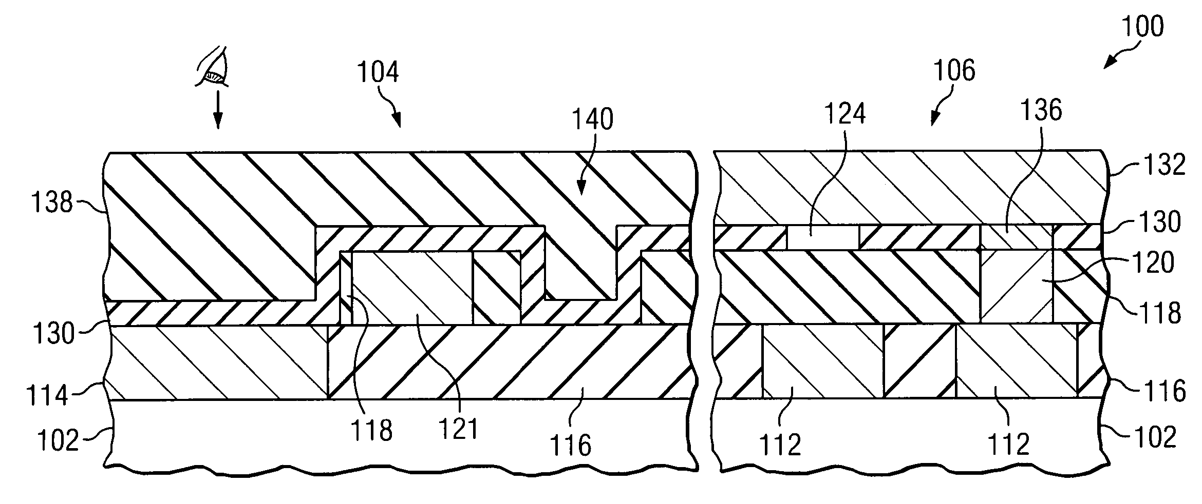
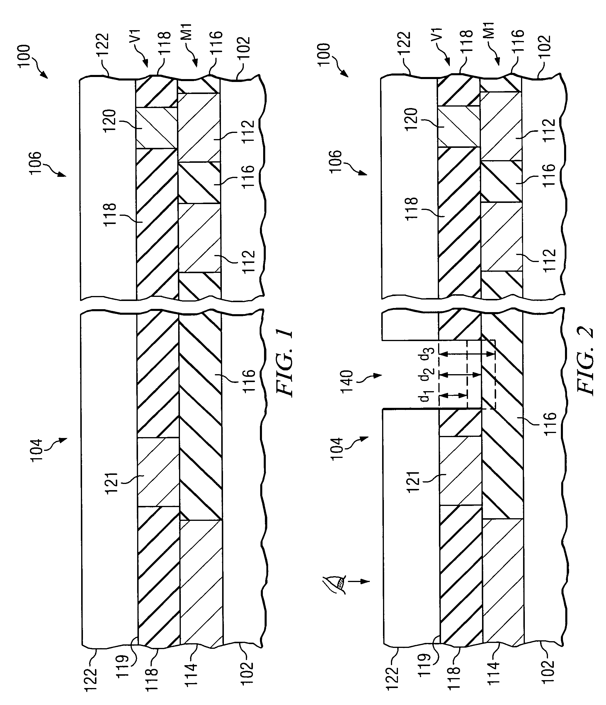
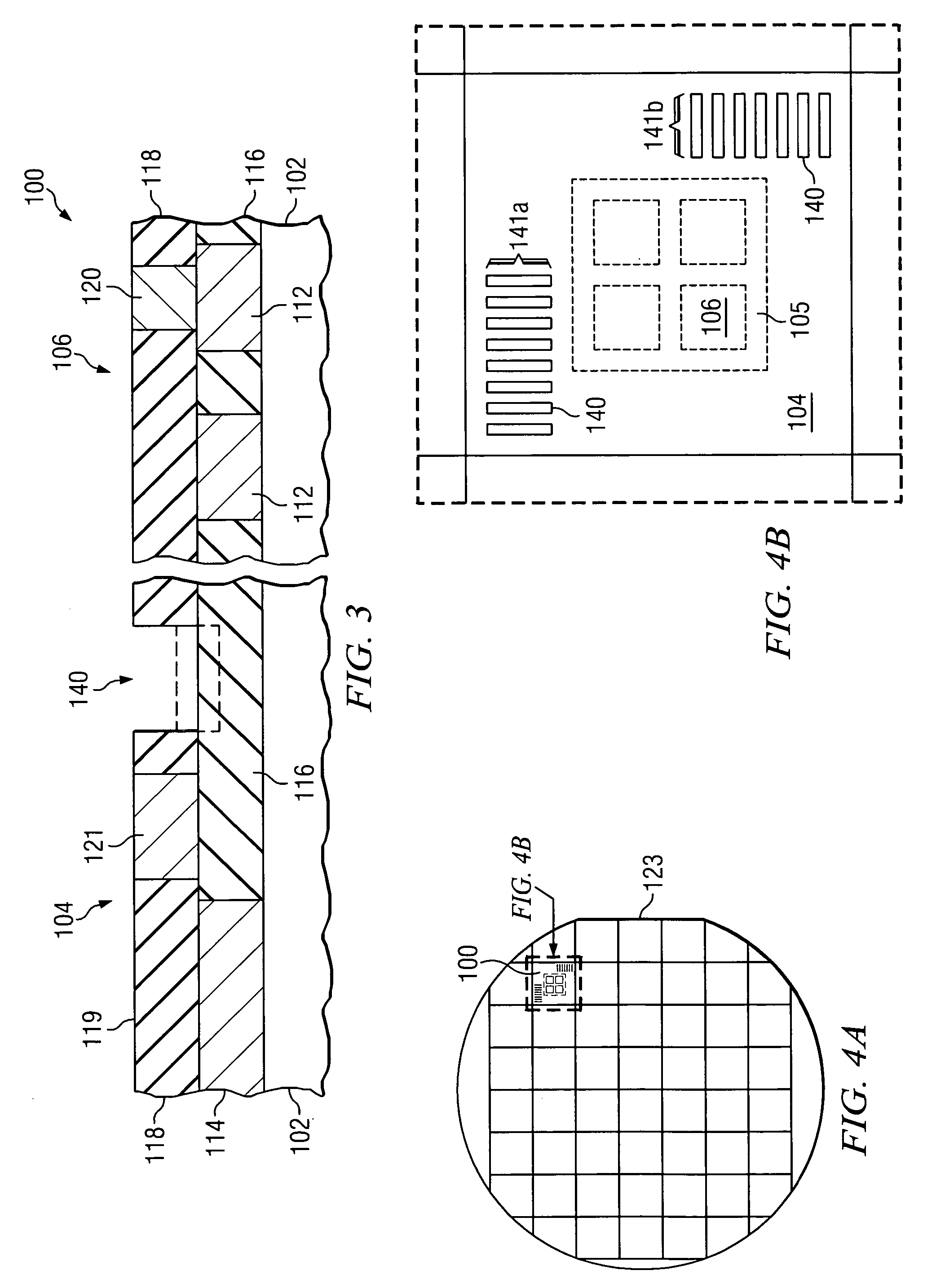
[0025]Embodiments of the present invention provide novel methods of forming alignment marks for the opaque MTJ stack of an MRAM device. With reference now to FIG. 1, there is shown a cross-sectional view of a semiconductor device 100 (also referred to herein as a die 100) comprising a workpiece 102. The workpiece 102 ma...


PUM


Abstract

A scheme for aligning opaque material layers of a semiconductor device. Alignment marks are formed in a via level of the semiconductor device. The alignment marks are formed using a separate lithography mask, and may have about the same length as vias formed in the via layer. The alignment marks comprise trenches that are not filled with material and are not exposed to a CMP process. An opaque material layer is deposited, and depressions are formed in the opaque material layer over the alignment mark trenches. The depressions in the opaque material layer are used to align a lithography process to open the opaque material layer over alignment marks in an underlying metallization layer. The alignment marks in the metallization layer are then used to align the lithography process used to pattern the opaque material layer.

Description

TECHNICAL FIELD[0001]The present invention relates generally to the fabrication of semiconductor devices, and more particularly to the alignment of opaque material layers of semiconductor devices.BACKGROUND[0002]Generally, semiconductor devices are fabricated by deposited a plurality of insulating, conductive and semiconductive material layers over a substrate or workpiece, and patterning the various material layers to form integrated circuits and electronic elements thereon. Each layer is typically aligned to an underlying material layer using alignment marks. The tools used to fabricate semiconductor devices visually locate the alignment marks, the position of which are programmed into the tools.[0003]If a material layer is transparent or translucent, as many insulating material layers and semiconductive material layers are, as well as photoresists or hard masks that are used as masks to pattern material layers, the tool can “see through” the insulating layer, semiconductor materi...

Claims


Application Information

Patent Timeline
Patent Type & Authority Patents(United States)
IPC IPC(8): H01L21/00H01L21/76H01L23/544
CPCH01L23/544H01L27/222H01L43/12H01L2223/5442H01L2223/54453H01L2924/0002H01L2223/54466H01L2223/5448H01L2924/00H10B61/00H10N50/01
Inventor SARMA, CHANDRASEKHAR
Owner POLARIS INNOVATIONS LTD
Why Eureka
Try Eureka