Dual damascene fabrication with low k materials

a technology of damascene and low k, applied in the field of semiconductor/solid-state device manufacturing, basic electric elements, electric apparatus, etc., can solve the problems of reducing the overall performance of the integrated circui

Inactive Publication Date: 2008-01-24
APPLIED MATERIALS INC
View PDF37 Cites 228 Cited by
  • Summary
  • Abstract
  • Description
  • Claims
  • Application Information

AI Technical Summary

Benefits of technology

[0012]The present invention generally provides methods and apparatuses for forming a dual damascene structure on the surface of a substrate. In one embodiment, the method includes depositing a dielectric film stack comprising a bottom barrier layer and a bulk dielectric insulating layer on the surface of the substrate, applying a first resist material layer over the dielectric film stack, performing trench lithography on the first resist material layer to form a trench pattern thereon, and etching the dielectric film stack until an desired etching depth to define one or more trenches therein according to the trench pattern on the first resist material layer. The method further includes removing the first resist material layer from the surface of the substrate, filling the one or more trenches with an organic material, depositing a mask layer over the organic material filling the one or more trenches, applying a second resist material layer over the mask layer, and performing via lithography on the second resist material layer to form a via pattern thereon. Then, the mask layer is etched to define one or more vias within the organic material filled trenches according to the via pattern on the second resist material layer. Further, the organic material and the bulk dielectric insulating layer are etched to form the one or more vias therein according to the via pattern. Still further, the method further includes etching the bottom barrier layer to form the one or more vias therein according to the via pattern and removing the organic material from the organic material filled trenches and the one or more vias. Thus, the one or more trenches and one or more vias are formed in the dielectric film stack on the surface of the substrate.
[0013]In another embodiment, a method of forming a dual damascene structure on the surface of a substrate having a bottom barrier layer, a bulk dielectric insulating layer, and a first resist material layer deposited thereon is provided. The method includes performing trench lithography on the first resist material layer to form a trench pattern thereon, etching the bulk dielectric insulating layer until an desired etching depth to define one or more trenches therein according to the trench pattern on the

Problems solved by technology

Integrated circuits have evolved into complex devices that can include millions of components (e.g., transistors, capacitors and resistors) on a single chip.
At sub-micron dimensions, capacitive coupling potentially occurs between adjacent metal interconnects, which may cause cross talk and/or resistance-capacitance (RC) delay and degrade the overall performance of the integrated circuit.
In addition, for high aspect ratios structures, the surfaces 161 of the resulting bottom of the via 111 are often very rough, contaminated with etched residues and damaged structures.
As a result, reliability of the fabricated device is severely affected.
In addition, as t

Method used


Image

  • Dual damascene fabrication with low k materials
  • Dual damascene fabrication with low k materials
  • Dual damascene fabrication with low k materials

Examples


Embodiment Construction

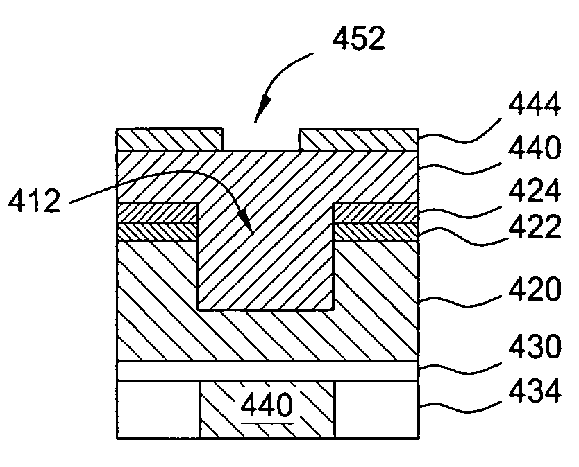
[0020]The present invention provides methods and apparatuses for fabricating a dual damascene structure on a substrate. First, trench lithography and trench patterning are performed on the surface of a substrate to etch a low-k dielectric material layer to a desired etch depth prior to forming of a via. The trenches are then filled with an organic fill material over the low-k dielectric material and a dielectric hard mask is deposited over the organic fill material prior to performing via lithography. A via resist pattern is then used to open the dielectric hard mask, which is in turn served as an etch mask to etch the organic fill material and form vias on the surface of the substrate. In contrast to other fabrication schemes having problems with etching the trenches, when etching the vias using methods of the invention, the trenches formed by the methods of the invention are protected by the organic fill material from being etched or damaged. A bottom etch stop layer on the bottom...


PUM


Abstract

The invention provides methods and apparatuses for fabricating a dual damascene structure on a substrate. First, trench lithography and trench patterning are performed on the surface of a substrate to etch a low-k dielectric material layer to a desired etch depth to form a trench prior to forming of a via. The trenches can be filled with an organic fill material and a dielectric hard mask layer can be deposited. Then, via lithography and via resist pattering are performed. Thereafter, the dielectric hard mask and the organic fill material are sequentially etched to form vias on the surface of the substrate, where the trenches are protected by the organic fill material from being etched. A bottom etch stop layer on the bottom of the vias is then etched and the organic fill material is striped. As a result, the invention provides good patterned profiles of the via and trench openings of a dual damascene structure.

Description

BACKGROUND OF THE INVENTION[0001]1. Field of the Invention[0002]Embodiments of the present invention generally relates to semiconductor processing technologies and, more specifically, to methods for fabricating a substrate containing dual damascene structures having low dielectric constant material thereon.[0003]2. Description of the Related Art[0004]Integrated circuits have evolved into complex devices that can include millions of components (e.g., transistors, capacitors and resistors) on a single chip. The demand for greater circuit density necessitates a reduction in the dimensions of the integrated circuit components, e.g., sub-micron dimensions and the use of various materials to fabricate devices in order to achieve much faster and better electrical performance, such as materials with higher conductivity used in metal lines, materials with lower permittivity (low-k) dielectric constant used as insulating materials, etc. For integrated circuit fabrication, metal interconnects ...

Claims


Application Information

Patent Timeline
IPC IPC(8): H01L21/44
CPCH01L21/31116H01L21/31138H01L21/31144H01L21/76835H01L21/76808H01L21/76834H01L21/31633H01L21/02118H01L21/02126H01L21/02167H01L21/022
Inventor NAIK, MEHUL
Owner APPLIED MATERIALS INC
Why Eureka
Try Eureka