Method and apparatus for identifying line-end features for lithography verification

a technology of lithography verification and feature identification, which is applied in the direction of instruments, computing, electric digital data processing, etc., can solve the problems of difficulty in identifying line-end features, distorting and more computationally expensive simulation of the final printed image of the circuit layout. achieve the effect of facilitating the identification of line-end features

Active Publication Date: 2007-03-20
SYNOPSYS INC
View PDF2 Cites 222 Cited by
  • Summary
  • Abstract
  • Description
  • Claims
  • Application Information

AI Technical Summary

Benefits of technology

[0008]One embodiment of the invention provides a system that facilitates identifying line-end features in a layout for an integrated circuit. The system operates by first receiving the layout for the integrated circuit. Next, the system selects a polygon from the layout and marks a line-end seed on the polygon. The system then determines if the line-end seed is associated with a line-end feature, and if so, the system marks the line-end feature.

Problems solved by technology

As semiconductor integration densities continue to increase at an exponential rate, circuits are becoming increasingly larger, which makes it more computationally expensive to simulate the final printed image for a circuit layout.
Furthermore, because of increasing integration densities, feature sizes are becoming increasingly smaller, which leads to problems with etch bias effects and optical proximity effects, which can distort the final printed image of a circuit layout.
Artifacts, such as serifs, which are generated by these correction operations, can cause difficulties in identifying line-end features.
Currently existing techniques for line-end detection suffer from low-precision when handling data with a high amount of noise, and from the difficulty in processing runs in directions such as 30 degrees and 45 degrees.
These difficulties largely arise because the artifacts introduced by etch bias correction and optical proximity correction tend to generate noise, which obscures the line-end features.

Method used


Image

  • Method and apparatus for identifying line-end features for lithography verification
  • Method and apparatus for identifying line-end features for lithography verification
  • Method and apparatus for identifying line-end features for lithography verification

Examples


Embodiment Construction

Data Flow

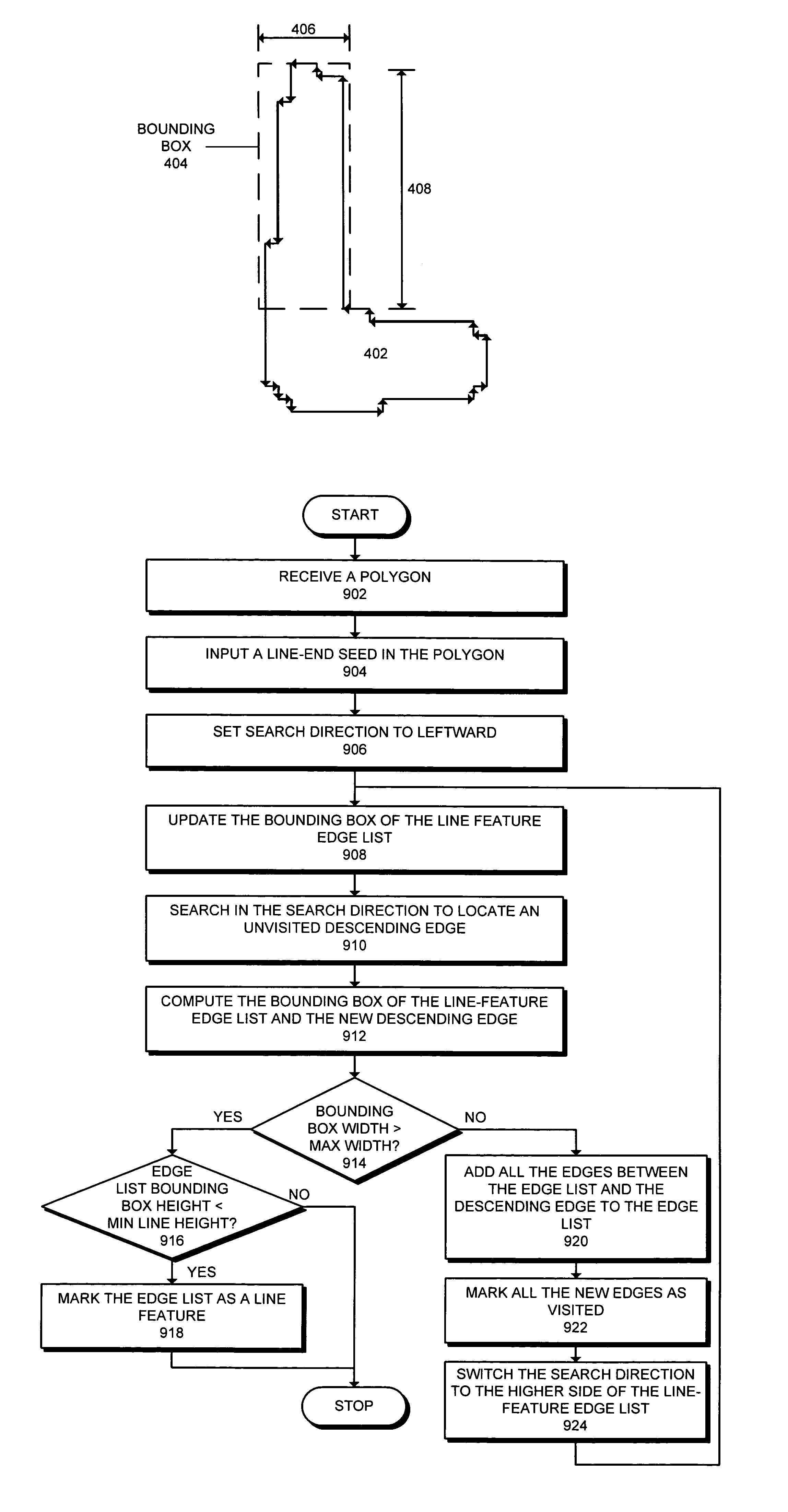
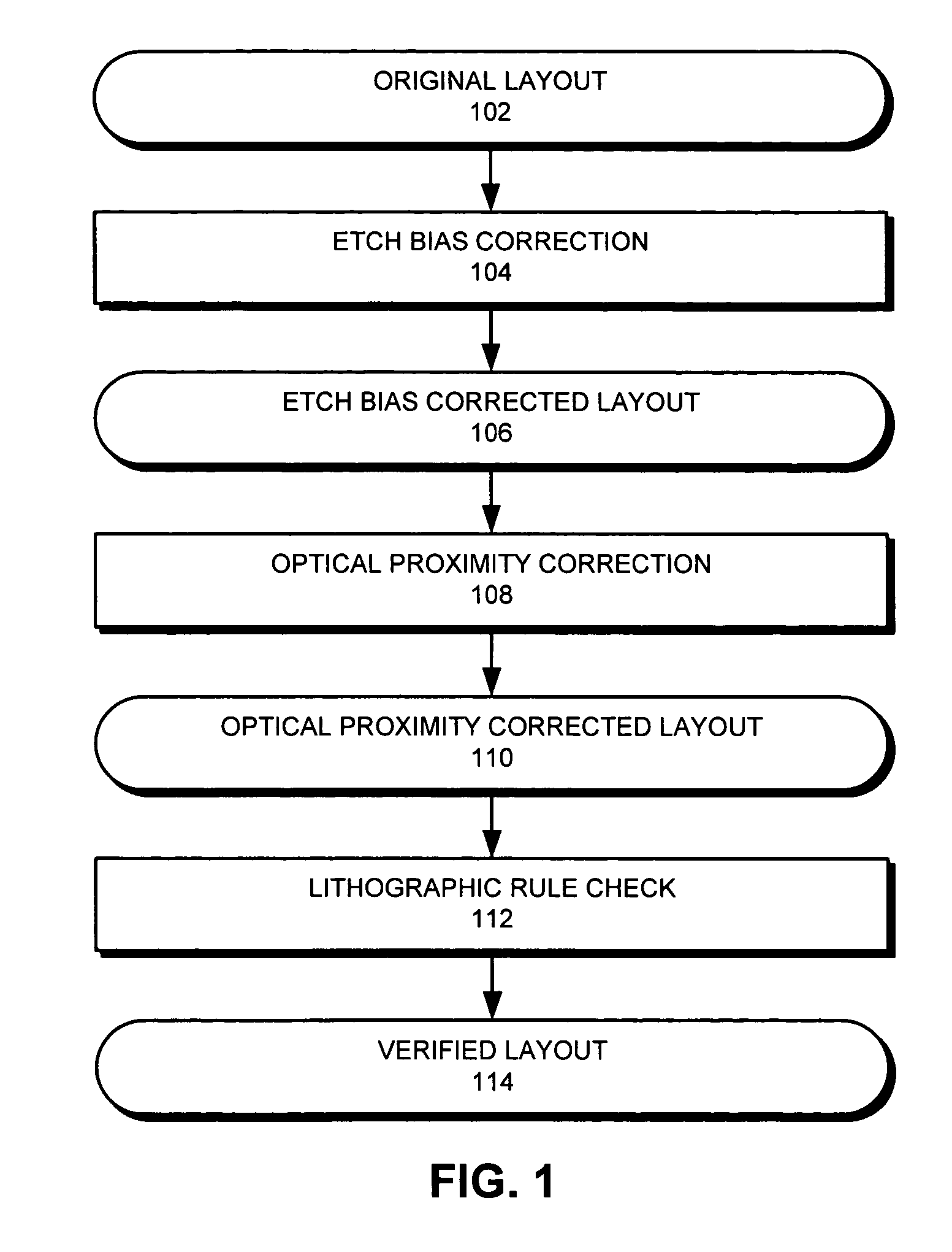
[0027]FIG. 1 illustrates a process flow in accordance with an embodiment of the invention. The system starts with original layout 102. Original layout 102 is then processed for etch bias correction 104 resulting in an etch-bias-corrected layout 106. Next, the etch-bias-corrected layout 106 is subjected to optical proximity correction 108 yielding optical-proximity-corrected layout 110. Optical-proximity-corrected layout 110 is then subjected to a lithographic rule check 112, which results in verified layout 114.

Artifacts Added by Corrections

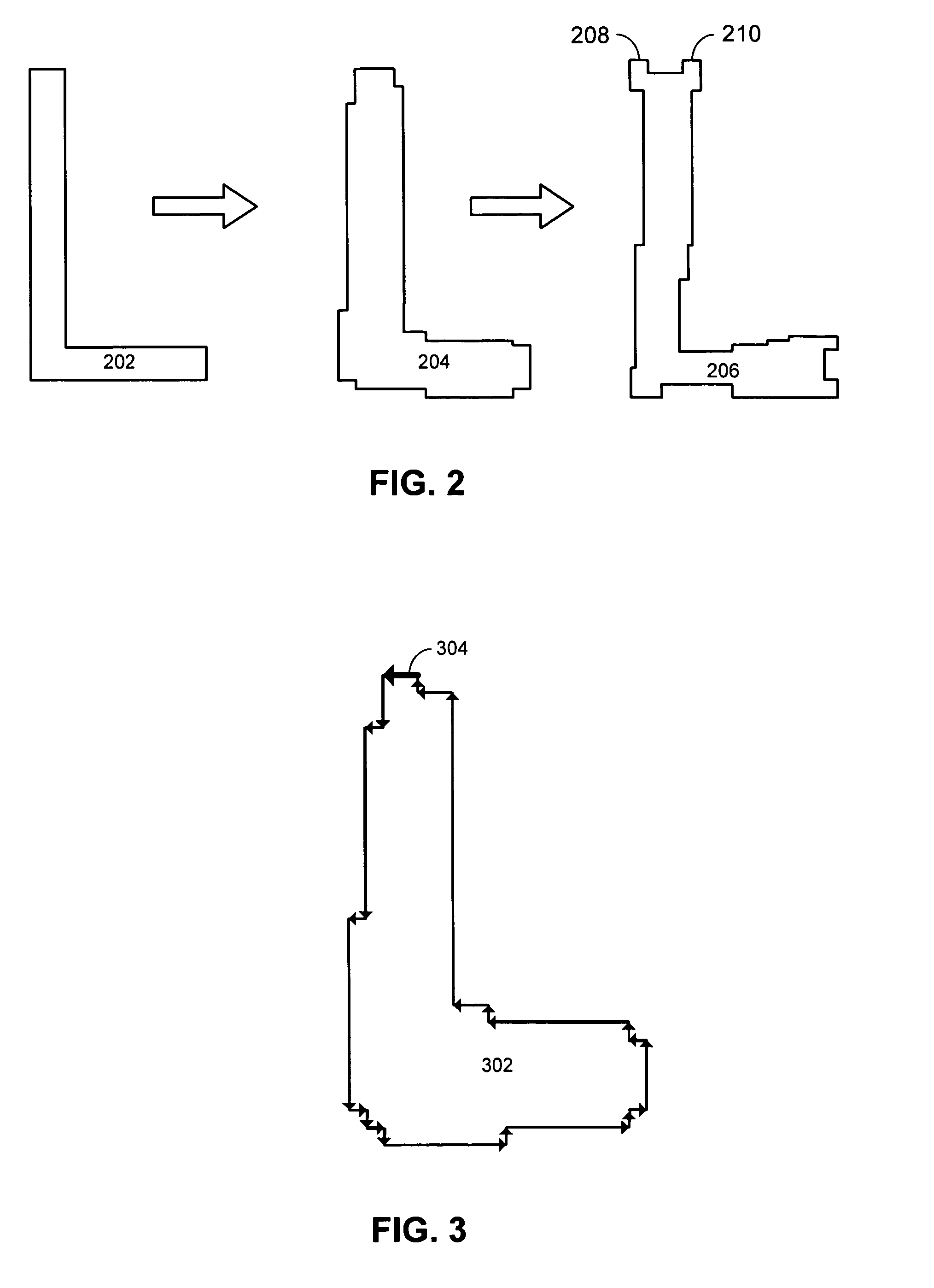
[0028]FIG. 2 illustrates artifacts added to a polygon during etch bias correction and optical proximity correction in accordance with an embodiment of the invention. A polygon 202 from original layout 102 is shown in FIG. 2. Note that identifying line-ends on polygon 202 is a straight-forward process and can be accomplished with relatively simple calculations.

[0029]The etch-bias correction process 104 transforms polygon 202 into polygon ...


PUM


Abstract

One embodiment of the invention provides a system that facilitates identifying line-end features in a layout for an integrated circuit. The system operates by first receiving the layout for the integrated circuit. Next, the system selects a polygon from the layout and marks a line-end seed on the polygon. The system then determines if the line-end seed is associated with a line feature, and if so, the system marks the line-end feature inside the line feature.

Description

BACKGROUND[0001]1. Field of the Invention[0002]The invention relates to techniques for verifying circuit layouts for semiconductor chips. More specifically, the invention relates to a method and an apparatus for identifying line-end features for lithography verification.[0003]2. Related Art[0004]As semiconductor integration densities continue to increase at an exponential rate, circuits are becoming increasingly larger, which makes it more computationally expensive to simulate the final printed image for a circuit layout. Consequently, such simulations are usually performed only for certain identified critical regions in the circuit based on the relative locations of specific features that are likely to cause problems, such as line ends.[0005]Furthermore, because of increasing integration densities, feature sizes are becoming increasingly smaller, which leads to problems with etch bias effects and optical proximity effects, which can distort the final printed image of a circuit layo...

Claims


Application Information

Patent Timeline
Patent Type & Authority Patents(United States)
IPC IPC(8): G06F17/50
CPCG06F17/5081G06F30/398
Inventor WU, JAMES XIAQING
Owner SYNOPSYS INC
Why Eureka
Try Eureka