Utilization of an ion gauge in the process chamber of a semiconductor ion implanter

a technology process chambers, which is applied in the field of ion gauges in the process chamber of semiconductor ion implants, can solve the problems of reducing the accuracy of pressure readings, destroying a portion of a resist layer formed on the wafer, and not being able to accurately count the number of ions (or atoms) leaving the ion gun

Inactive Publication Date: 2006-03-07
POLARIS INNOVATIONS LTD
View PDF39 Cites 5 Cited by
  • Summary
  • Abstract
  • Description
  • Claims
  • Application Information

AI Technical Summary

Problems solved by technology

Specifically, it is not possible to accurately count the number of ions (or atoms) leaving the ion gun.
When the ions hit the semiconductor wafer, they may destroy a portion of a resist layer formed on the wafer.
However, this location reduces the accuracy of the pressure reading for two reasons.
First, resist outgassing causes dramatic increase of pressure near the wafer.
That is, the high energy of arsenic causes a lot of resist outgassing, and hence a large pressure increases.
However, nitrogen implantation causes a substantial amount of resist outgassing and beam neutralization, which are not detected by the ion gauge in its current location.
A high pressure compensation value exposes the process to a non-acceptable risk of dose error.
The risk stems from the pressure read out variability and instability that are inherent in any ion gauge.
Experience has shown that for very high P-COMP values, it is difficult to repeatedly produce wafers with the same dosing.
In this manner, there are not enough electrons to appreciably neutralize the ion beam.
However, reducing the beam current lowers the throughput of the implanter and reduces the tool capacity.

Method used


Image

  • Utilization of an ion gauge in the process chamber of a semiconductor ion implanter
  • Utilization of an ion gauge in the process chamber of a semiconductor ion implanter
  • Utilization of an ion gauge in the process chamber of a semiconductor ion implanter

Examples


Embodiment Construction

[0034]Reference will now be made in detail to the preferred embodiments of the present invention, examples of which are illustrated in the accompanying drawings, wherein like reference numerals refer to like elements throughout.

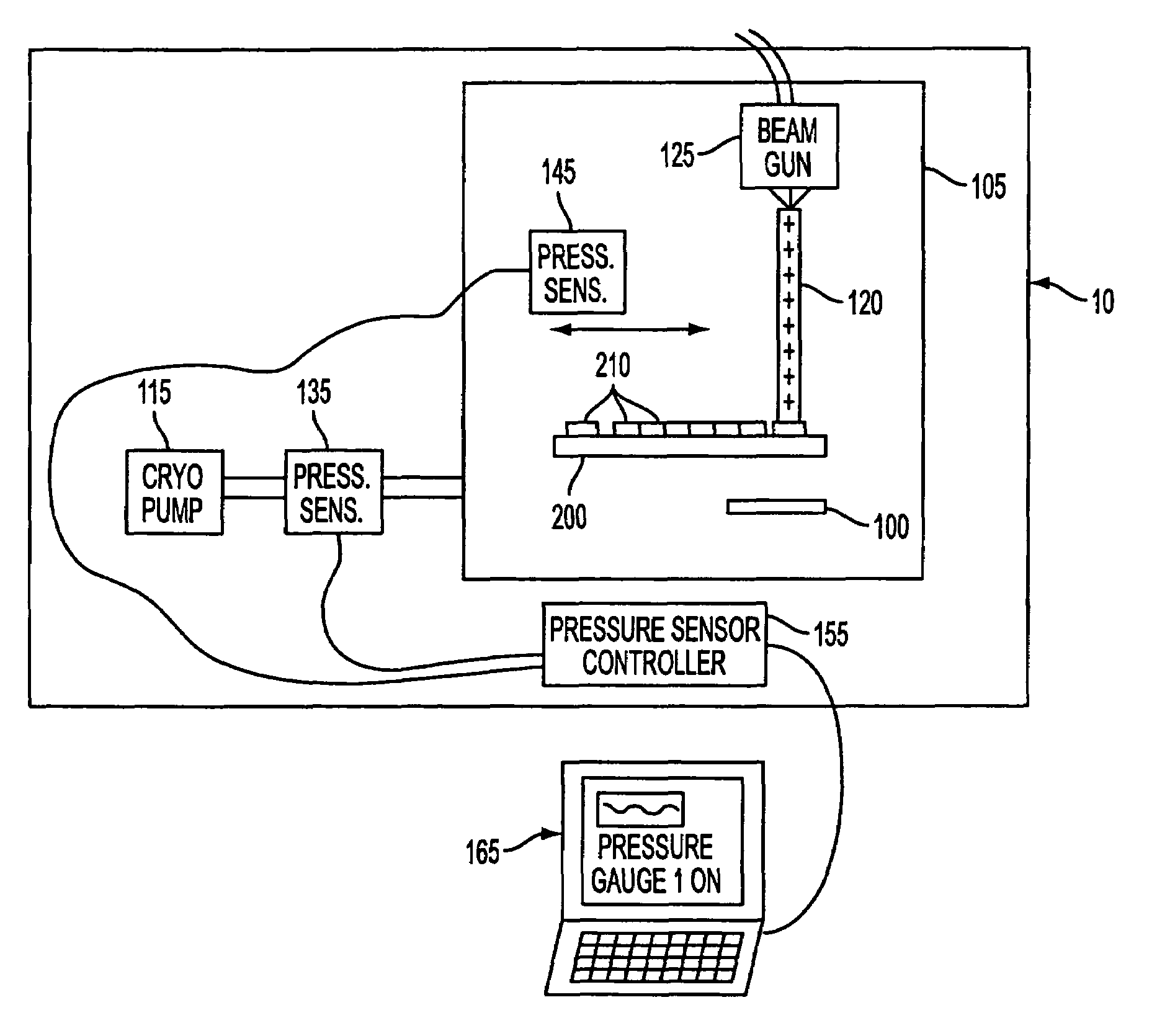
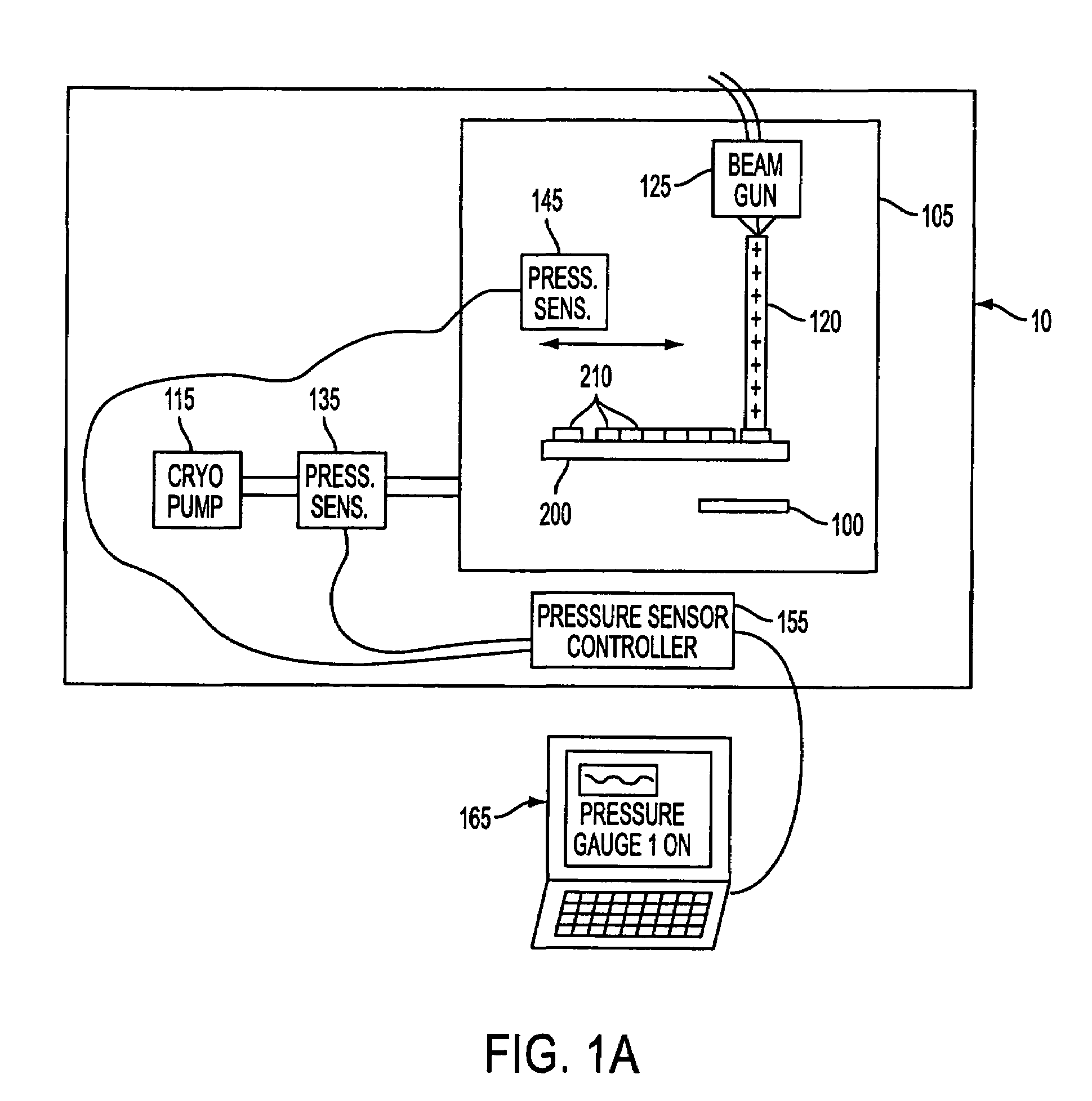
[0035]FIG. 1A is a schematic side view of an ion implanter 10. The implanter may be an Axcelis GSD™ platform implanter. The implanter has a chamber 105, which is kept at a very low pressure by cryo pumps, one of which is represented by reference numeral 115. Within the chamber 105, a beam gun 125 produces an ion beam 120 which is focused on wafers 210. The wafers 210 are placed around a disk 200. A faraday 100 is provided under the disk 200 to sense beam current. A first pressure sensor 135 is provided outside of the chamber 105 in the vicinity of the cryo pump 115. This location corresponds with a conventional location and is useful for implanting ions that produce a large pressure response during resist outgassing. A second pressure sensor 145 is provided w...


PUM


Abstract

A device to implant impurities into a semiconductor wafer has a process chamber having a wall, a pressure compensation unit, a disk to support a plurality of semiconductor wafers within the process chamber. The disk has a radially extending slot arranged among the wafers. A beam gun is positioned within the process chamber to shoot an ion beam at the semiconductor wafers. A cryo pump minimizes the pressure within the process chamber. A first ion gauge is positioned between the process chamber and the cryo pump. A second ion gauge extends through the wall of the process chamber. A switching device selectively connects the first or second ion gauge to the pressure compensation unit. A faraday receives ions from the ion gun filter after the ions travel through the slot in the disk. A current meter counts the number of electrons flowing to the disk faraday to neutralize the ions.

Description

BACKGROUND OF THE INVENTION[0001]Impurities are implanted into semiconductor devices for a variety of reasons, including introducing electrons and holes into the semiconductor substrate in order to locally change the conductive properties of the substrate. For example, silicon has four electrons in the outer ring. Phosphorus has five electrons in its outer ring, one more than silicon. Boron has three electrons in its outer ring, one fewer electron than silicon. Boron can be used to introduce holes into the substrate. Phosphorous can be used to introduce electrons into the substrate.[0002]To enable implantation, the impurities are implanted as ions having one fewer electron than the neutral species. During the implantation process, the electron deficit can be used to determine how much impurity has been implanted. Specifically, it is not possible to accurately count the number of ions (or atoms) leaving the ion gun. Therefore, a predetermined portion of the ions is directed to an ion...

Claims


Application Information

Patent Timeline
Patent Type & Authority Patents(United States)
IPC IPC(8): G21K5/10H01J37/317
CPCH01J37/3171H01J2237/004H01J2237/31705H01J2237/30455H01J2237/31703H01J2237/18
Inventor GARZA, FREDERICOWRIGHT, MICHAELPETERSON, KARL
Owner POLARIS INNOVATIONS LTD
Why Eureka
Try Eureka