Semiconductor switching device

a switching device and semiconductor technology, applied in the direction of overvoltage protection resistors, emergency protective arrangements for limiting excess voltage/current, pulse techniques, etc., can solve the problems of semiconductor element breakdown, semiconductor switching device as a whole becomes complicated, and the manufacturing cost of semiconductor elements rises, etc., to achieve safe and reliable semiconductor switching devices

Inactive Publication Date: 2006-03-07
MITSUBISHI ELECTRIC CORP
View PDF12 Cites 6 Cited by
  • Summary
  • Abstract
  • Description
  • Claims
  • Application Information

AI Technical Summary

Benefits of technology

[0017]In the semiconductor switching device according to the first aspect of the present invention, overvoltage caused by asynchronous turn on / off among the semiconductor switching elements can be absorbed into the snubber circuit and, at the same time, loss at the snubber circuit can be reduced. Moreover, even if voltage of power source rises by an accident such as short circuit in a load connected thereto to raise divided voltage of the semiconductor switching element, the semiconductor switching element as well as the snubber circuit is protected and never be broken.
[0020]In the semiconductor switching device according to the third aspect of the present invention, even if one or more semiconductor switching element is broken so that divided voltage of the other semiconductor switching element rises and, in addition, some accident happens so that the voltage of power source rises, thermal heat at the first controlling semiconductor element can be reduced by enlarging impedance of the first impedance element to reduce current flowing into the non-linear unit or by increasing the number of the first controlling semiconductor elements to reduce thermal heat for each first controlling semiconductor element. Thereby, the first controlling semiconductor element is protected from to be broken.
[0024]In the semiconductor switching element in which large number of the semiconductor switching elements are connected in series, the leakage current of each semiconductor switching element is uneven so that the normal divided voltage for each semiconductor switching element is also uneven. Therefore, the semiconductor switching device according to the fifth aspect of the present invention compensates this unevenness of the leakage current to equalize the normal divided voltage among the semiconductor switching elements. The normal divided voltage for the semiconductor switching element of larger leakage current is lower and the normal divided voltage for the semiconductor switching element of smaller leakage current is higher. The non-linear units detects this higher normal divided voltage and draw current therethrough additionally to the leakage current through the semiconductor switching element.
[0039]With the diode-on delay device, beginning of conduction at the first diode is delayed so that all the semiconductor switching elements turns on before current starts to flow through the first diode and first capacitor. Thereby, current bypassing the semiconductor switching element of late turn on does not flows so that clue to the reverse current does not happens. Accordingly, safe and reliable semiconductor switching device can be obtained regardless of the asynchronous turn on among the semiconductor switching elements.

Problems solved by technology

Firstly, overvoltage is caused by asynchronous turn on / off operation among the semiconductor switching elements.
Secondly, overvoltage is also caused by inductance of circuits connected thereto.
Thirdly, in a semiconductor switching device in which semiconductor switching elements are connected in series, leakage current of each semiconductor switching element probably varies so that divided voltage for each semiconductor switching element also varies.
Moreover, in case a semiconductor switching device is constructed from a large number of semiconductor switching elements 2 connected in series and parallel, a power supply 33 for a gate drive circuit 12 is required for each semiconductor element 2 so that the semiconductor switching device as a whole becomes complicated and manufacturing cost thereof rises.
However, if the voltage of the first capacitor 5 is set too high, protection for the semiconductor elements 2 becomes insufficient so that breakdown of the semiconductor elements 2 may be caused.
Furthermore, especially in a semiconductor switching device in which a large number of the semiconductor switching elements 2 are connected in series to convert very high voltage, a power supply 33 to supply adequate voltage for a gate drive circuit 12 of each semiconductor switching element 2 becomes complicated and costly.

Method used


Image

  • Semiconductor switching device
  • Semiconductor switching device
  • Semiconductor switching device

Examples


embodiment 1

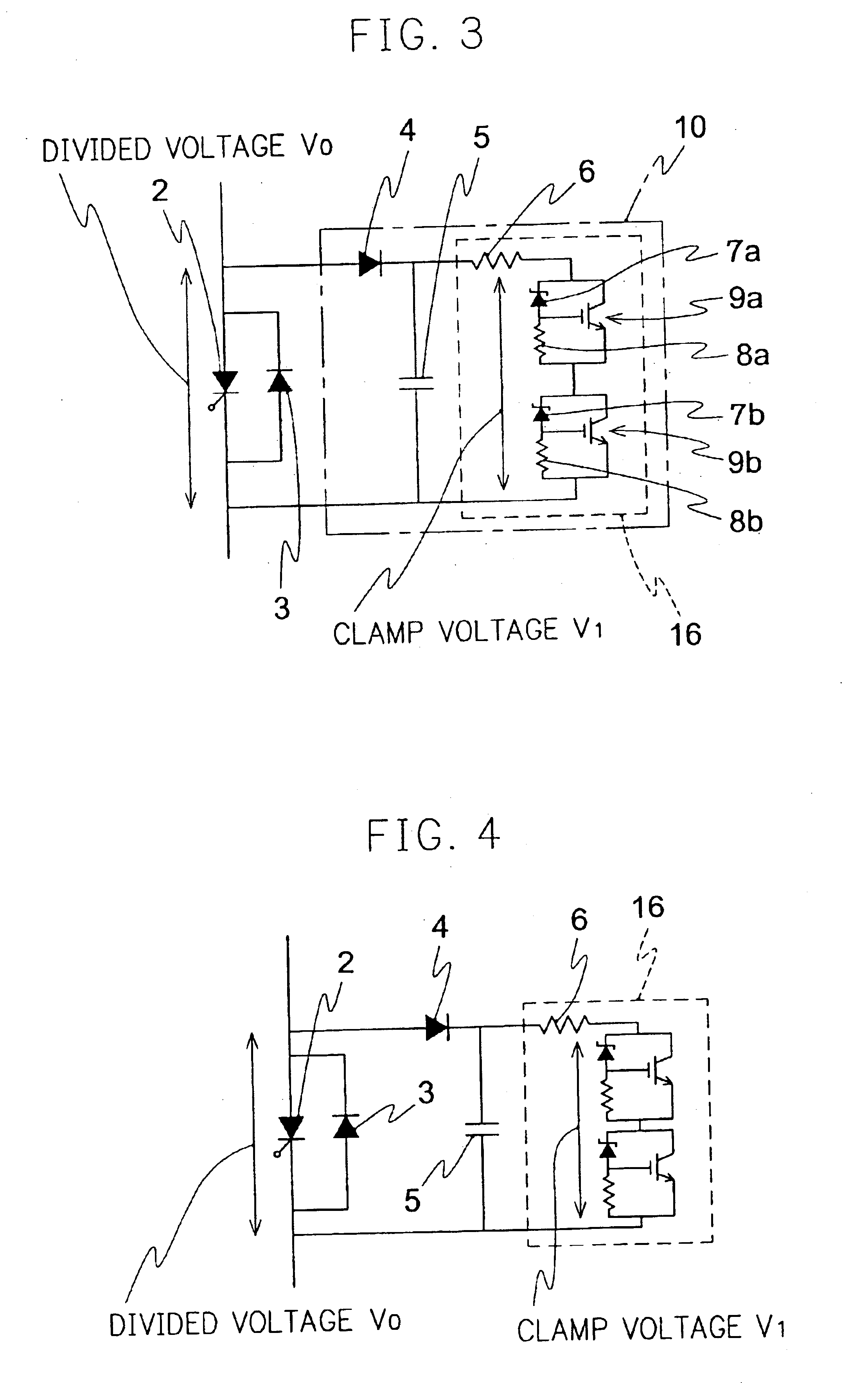
[0071]Embodiment 1 of the present invention is described with referring to FIG. 3. A unit in a bridge arm of a semiconductor switching device of the present invention, that is, a series valve with an auxiliary circuit thereof, is shown in FIG. 3. In FIG. 3, 10 denotes a snubber circuit, 16 denotes a non-linear circuit, 4 denotes a first diode, 5 denotes a first capacitor, 6 denotes a first impedance element, 7(7a, 7b) denotes a first Zener diode which is a non-linear resistor element, 8(8a, 8b) denotes a first resistor, 9(9a, 9b) denotes a first controlling semiconductor element, V1 denotes a clamp voltage determined by the first Zener diodes 7a, 7b of the non-linear circuit 16, 2 denotes a semiconductor switching element, 3 denotes a reverse-conducting diode connected parallelly and reversely to the semiconductor switching element 2, and V0 denotes normal divided voltage in which the semiconductor switching element 2 operates. While a IGBT (Insulated Gate Bipolar Transistor) is sho...

embodiment 2

[0082]Embodiment 2 of the present invention is described with referring to FIG. 4. As described above, an accident, such as a short circuit in electric facilities, happens at the supplying side of the semiconductor switching device, voltage of power source rises. As the result of our researches and experiments for various power sources, we have found that the voltage, under the accident, rises to about 1.27 times as high as that without accident at the maximum. Therefore, the clamp voltage V1 is set to be about 1.3 times or higher to the normal divided voltage V0.

[0083]With the clamp voltage V1 about 1.3 times or larger to the normal divided voltage V0, the non-linear circuit 16 is protected from the destruction even the accident happens at the supplying side. Moreover, the clamp voltage V1 can be set to its minimum necessity voltage. In case the clamp voltage V1 is set to about 1.3 times as high as the normal divided voltage V0, the clamp voltage V1 is minimized so that breakdown o...

embodiment 3

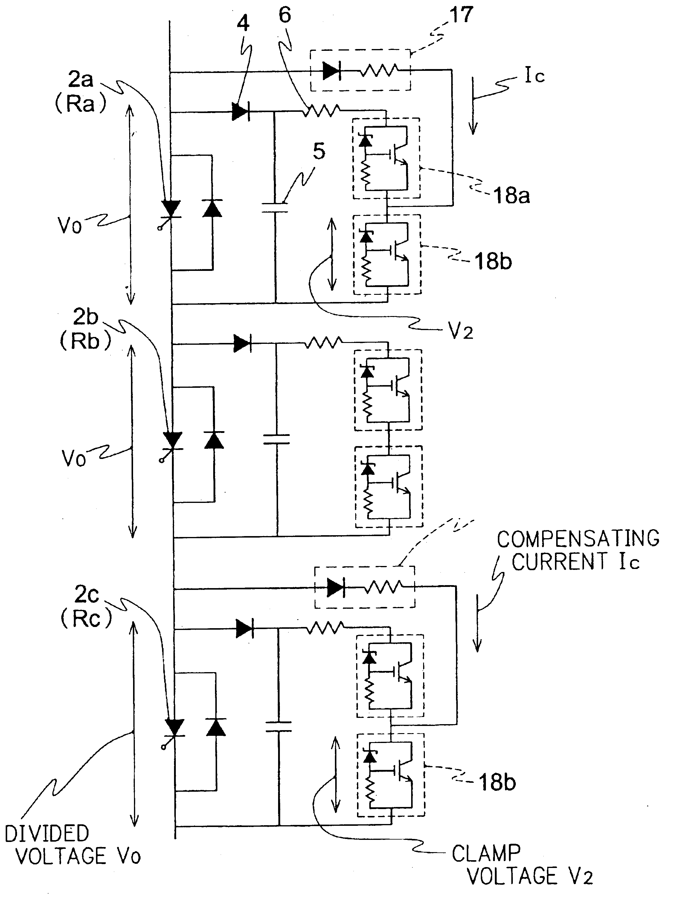
[0084]Embodiment 3 of the present invention is described with referring to FIG. 5. As described above, the divided voltage of the semiconductor switching element 2 is higher than the normal divided voltage V0 when the accident happens. As the divided voltage exceeds the clamp voltage V1, current flows through the non-linear circuit 16 and loss, which depends on the current and the clump voltage V1, is caused at the first controlling semiconductor element 9a, 9b. If the loss exceeds the capacity of the first controlling semiconductor element 9a, 9b thermally, the first controlling semiconductor element 9a, 9b is broken. To protect the first controlling semiconductor element 9a, 9b, impedance of the first impedance element 6 is increased in the present Embodiment so that current flowing through the non-linear circuit 16 is decreased, and thereby, the loss at the first controlling semiconductor element 9a, 9b is suppressed below the capacity thereof. At this time, impedance of the firs...


PUM


Abstract

Self-quenching switching elements are connected in series in a semiconductor switching device. Snubber circuits including a diode, a capacitor, and a non-linear circuit are connected in parallel with the respective semiconductor switching elements. In the snubber circuit, the diode and the capacitor are connected in series, and the non-linear circuit is connected in parallel with the capacitor. The non-linear circuit includes an impedance element, a Zener diode, and a controlling semiconductor element and draws current through the controlling semiconductor element when applied voltage exceeds the Zener voltage of the Zener diode. The Zener voltage is larger than a divided voltage applied to the semiconductor element during a fault in a power system.

Description

FIELD OF THE INVENTION[0001]The present invention relates to a semiconductor switching device used, for example, for a converter in a power system to convert AC to DC and vise versa.BACKGROUND OF THE INVENTION[0002]A conventional semiconductor switching device, such as described in Japanese Unexamined Patent Publication No. 33,001 / 1999, is shown in FIG. 26. Although a semiconductor switching device typically comprises semiconductor switching elements connected in series and parallel, only one of them is shown in FIG. 26. As shown in FIG. 26, a reverse-conducting diode 3 is connected to a semiconductor switching element 2 to produce a reverse-conducting switching element 1. Moreover, a snubber circuit 10 is connected to the reverse-conducting switching element 1. In a semiconductor switching device in which reverse-conducting switching elements 1 are connected in series and parallel, each reverse-conducting switching element 1 is called a series valve and each reverse-conducting swit...

Claims


Application Information

Patent Timeline
Patent Type & Authority Patents(United States)
IPC IPC(8): H02H3/20H02H9/04H02H7/12H02H7/20H02M1/00H02M1/08H03K17/0814H03K17/16H03K17/56
CPCH03K17/08144H02M1/08H03K17/105
Inventor ITO, HIROSHIIWATA, AKIHIKOSUZUKI, AKIHIRO
Owner MITSUBISHI ELECTRIC CORP
Why Eureka
Try Eureka