
Non-volatile semiconductor memory array and method of reading the same memory array

Inactive Publication Date: 2006-03-07
HITACHI LTD +1
View PDF12 Cites 5 Cited by
  • Summary
  • Abstract
  • Description
  • Claims
  • Application Information

AI Technical Summary

Benefits of technology

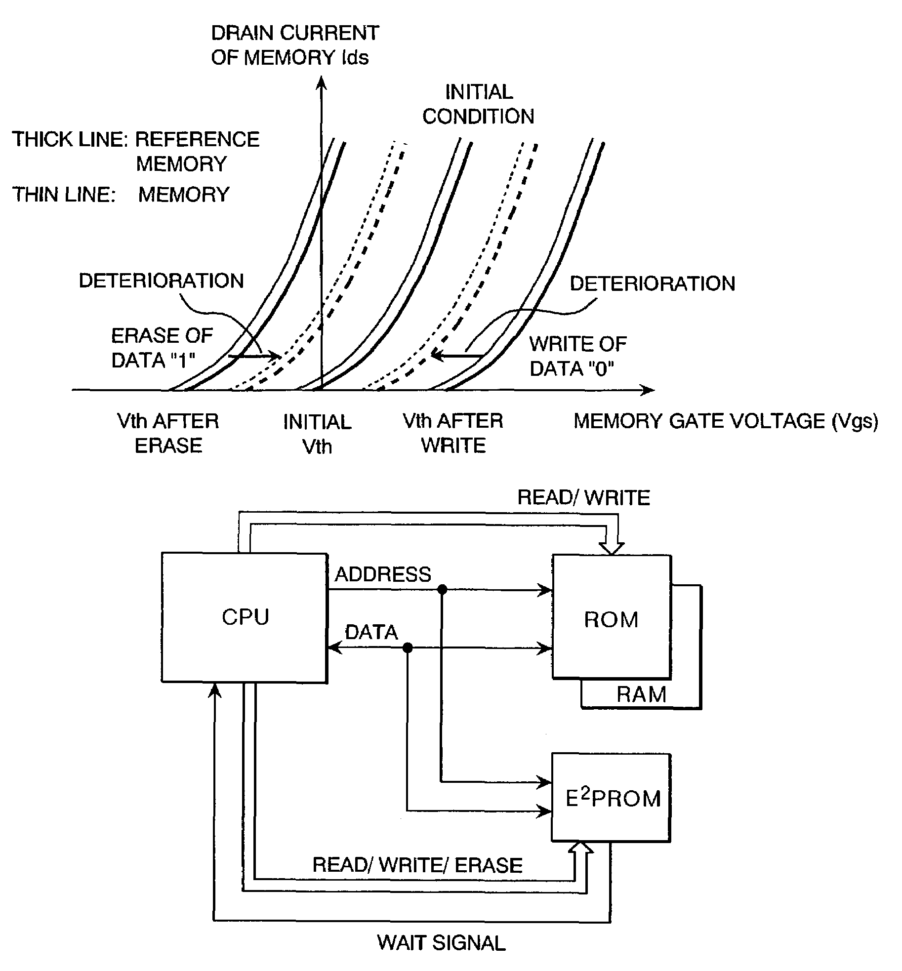
[0009]It is therefore an object of the present invention to provide a non-volatile semiconductor memory array provided with a read timing generation circuit which can solve the problems explained above that there are restrictions on the number of times of reprogram operations, application years and read time and can vary the read timing of the memory depending on the number of times of reprogram operation and application years of the relevant memory by generating a wait signal to control the read timing.

Problems solved by technology

Therefore, an electrically reprogrammable EEPROM is limited in the number of times of reprogram operations and in the application years.
Moreover, the number of times of reprogram operation and application years of EEPROM have been restricted with deterioration of Vth and limitation on the read time.
When the number of times of reprogram operation and application years are small in the electrically reprogrammable EEPROM, here lies a problem that a read operation rate is rather low due to the specification of fixed read period assuming deterioration of Vth of memory transistor while the read operation can be executed at a high speed.

Method used


Image

  • Non-volatile semiconductor memory array and method of reading the same memory array
  • Non-volatile semiconductor memory array and method of reading the same memory array
  • Non-volatile semiconductor memory array and method of reading the same memory array

Examples


Embodiment Construction

[0028]The like elements are designated with the like reference numerals throughout the drawings of embodiments.

[0029]A semiconductor memory array block of the first embodiment of the present invention is illustrated in FIG. 8. As can be understood from the prior art of FIG. 2, reference memories are allocated within a block. According to an example of FIG. 8, a DM0 reference memory allocated in the most significant bit of an X decoder is simultaneously reprogrammed or erased whenever the memory in the block is reprogrammed or erased. In order to reprogram and erase the relevant reference memory as explained above, the word line exclusive for the reference memory, reference memory transistor gate control line, reference memory bit line and reference memory source line are controlled. Thereby, the reference memory DM0 is always set to erase “1” state.

[0030]This profile will be explained with the status transition diagrams of FIG. 9 (a) and FIG. 9 (b). In FIG. 9 (a), a memory is shifte...


PUM


Abstract

A non-volatile semiconductor memory EEPROM is usually deteriorated depending on the number of times of program and erase operations and application years thereof. A read operation rate of the EEPROM is generally specified to the operation rate considering deterioration of memory and even in the case where the number of times of program and erase operations is rather small and application years are also rather small, the read operation has been conducted at the read operation rate specified considering deterioration of memory. Moreover, when deterioration of memory is advanced exceeding the specified deterioration, the read operation is now disabled in the worst case. In order to overcome such problem, the reference memories are allocated for every erase and program unit block in the EEPROM memory array, the reference memories are also programmed and erased whenever the memories in the block are erased and programmed and the read timing of memory is generated from the read timing of these reference memories. Moreover, the read timing of the reference memories is outputted as an external interface.

Description

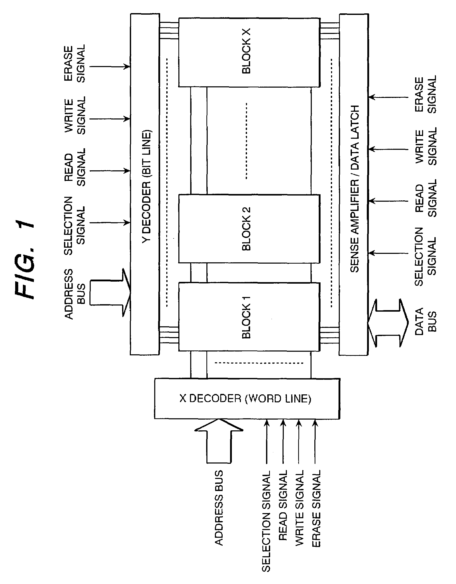
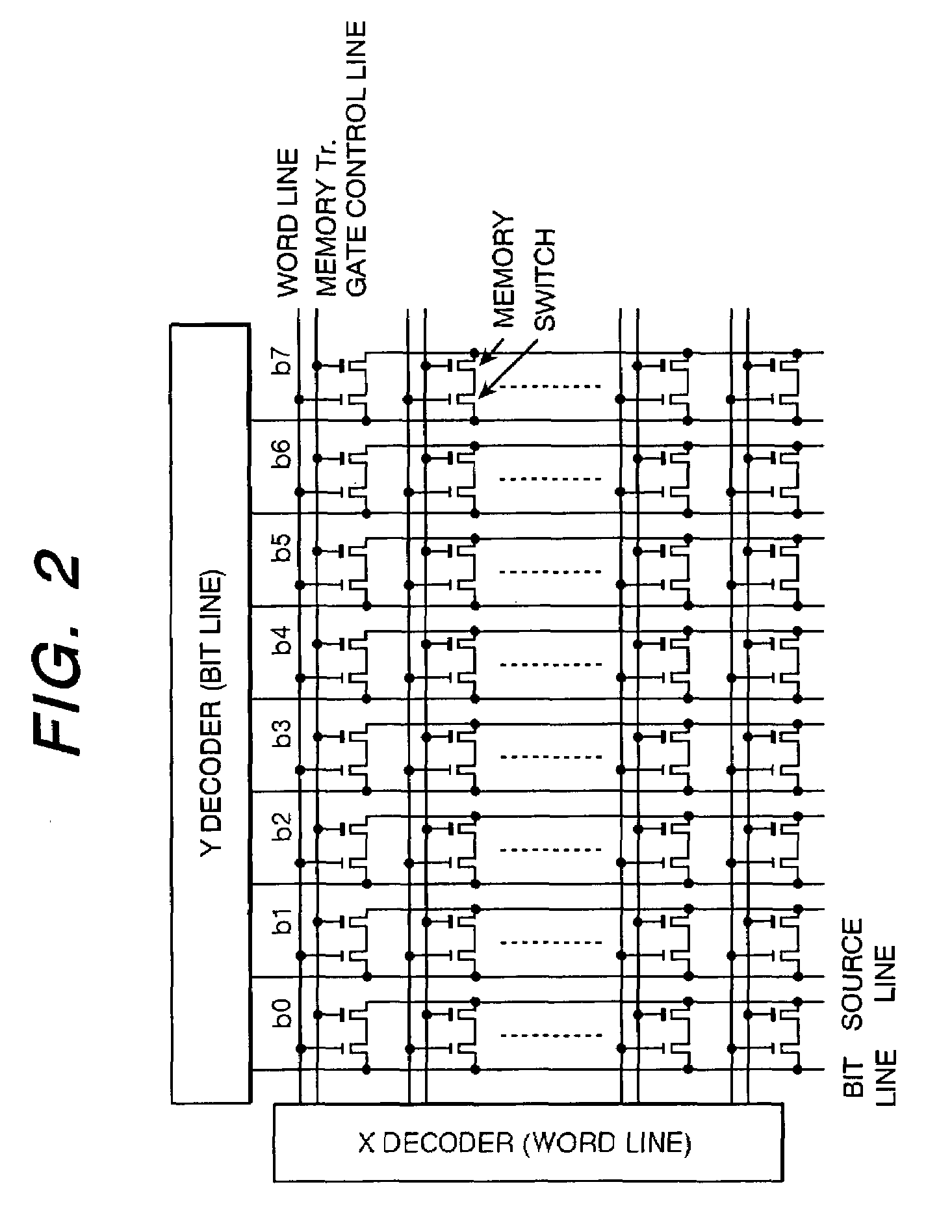
FIELD OF THE INVENTION[0001]The present invention relates to reference memories provided in a non-volatile semiconductor memory array to conduct erase and program operations and particularly to a method of reading a memory by utilizing the reference memories in the memory array.BACKGROUND OF THE INVENTION[0002]An example of structure of memory array of the existing electrically erasable and programmable ROM (EEPROM) is illustrated in FIG. 1. As illustrated in FIG. 1, a memory array is formed of a plurality of blocks, each of which is consisting of a unit block for erase and program operation. FIG. 2 illustrates a layout of the internal circuit of block. Each block is usually composed of one byte (8 bits) to a plurality of bytes. In the case of EEPROM, one bit is composed of a switch transistor and a memory transistor. FIG. 2 illustrates a block of the one byte structure.[0003]A structure of the MONOS (Metal Oxide Nitride Oxide Semiconductor) type EEPROM and concept of erase and prog...

Claims


Application Information

Patent Timeline
IPC IPC(8): G11C16/00G06F12/00G11C16/02G11C16/04G11C16/06
CPCG11C16/32G11C16/26
Inventor YAMAZOE, TAKANORIYOSHIGI, HIROSHIKANAI, TAKEO
Owner HITACHI LTD
Learn More