Reducing discontinuities in segmented imaging sensors
a segmented imaging and discontinuity technology, applied in the field of electronic imaging sensors, can solve the problems of discontinuities at the sensor segment, unfavorable increase in processing time merely, and discontinuities formed at the boundary between each segment, so as to achieve the effect of reducing discontinuities
- Summary
- Abstract
- Description
- Claims
- Application Information
AI Technical Summary
Benefits of technology
Problems solved by technology
Method used
Image

Examples
first embodiment
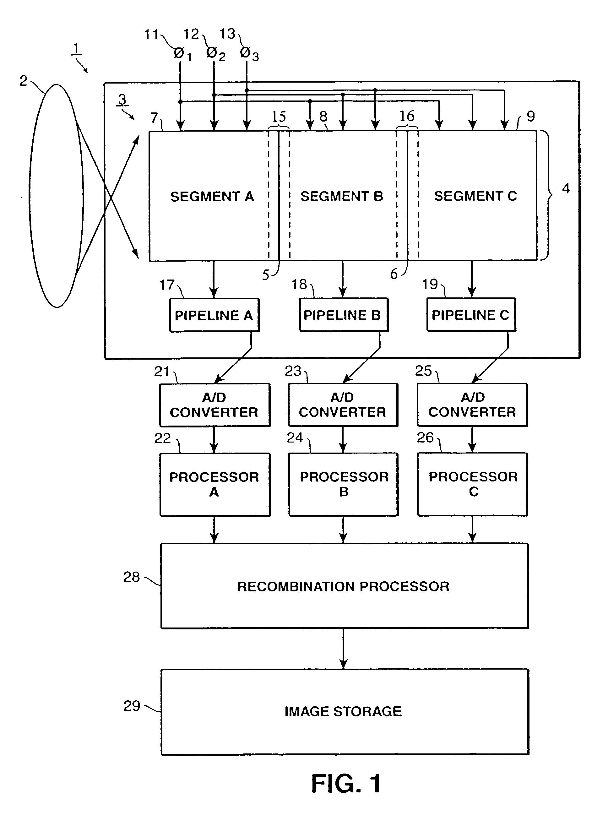
[0036]FIG. 2 is a representational view of a first embodiment of an electronic imaging sensor according to the invention.
[0037]Briefly, according to the first embodiment, an electronic imaging sensor includes a sensor array segmented into plural disjoint segments, a respective plurality of output pipelines, each of which corresponds to each of the plural segments of the sensor array, and circuitry for duplicating image data for an overlap region at each boundary between segments. The circuitry includes charge or voltage duplicating circuitry that obtains multiple outputs for each pixel in the overlap region. The duplication circuitry provides each of the multiple outputs to individual ones of the output pipelines that border on the overlap region.
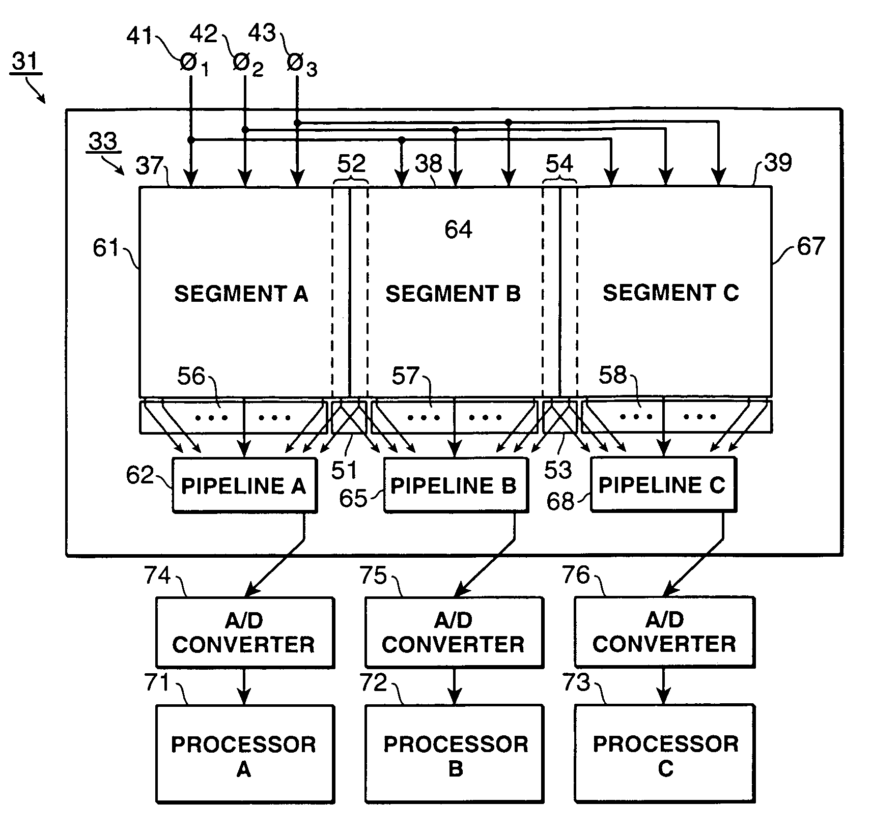
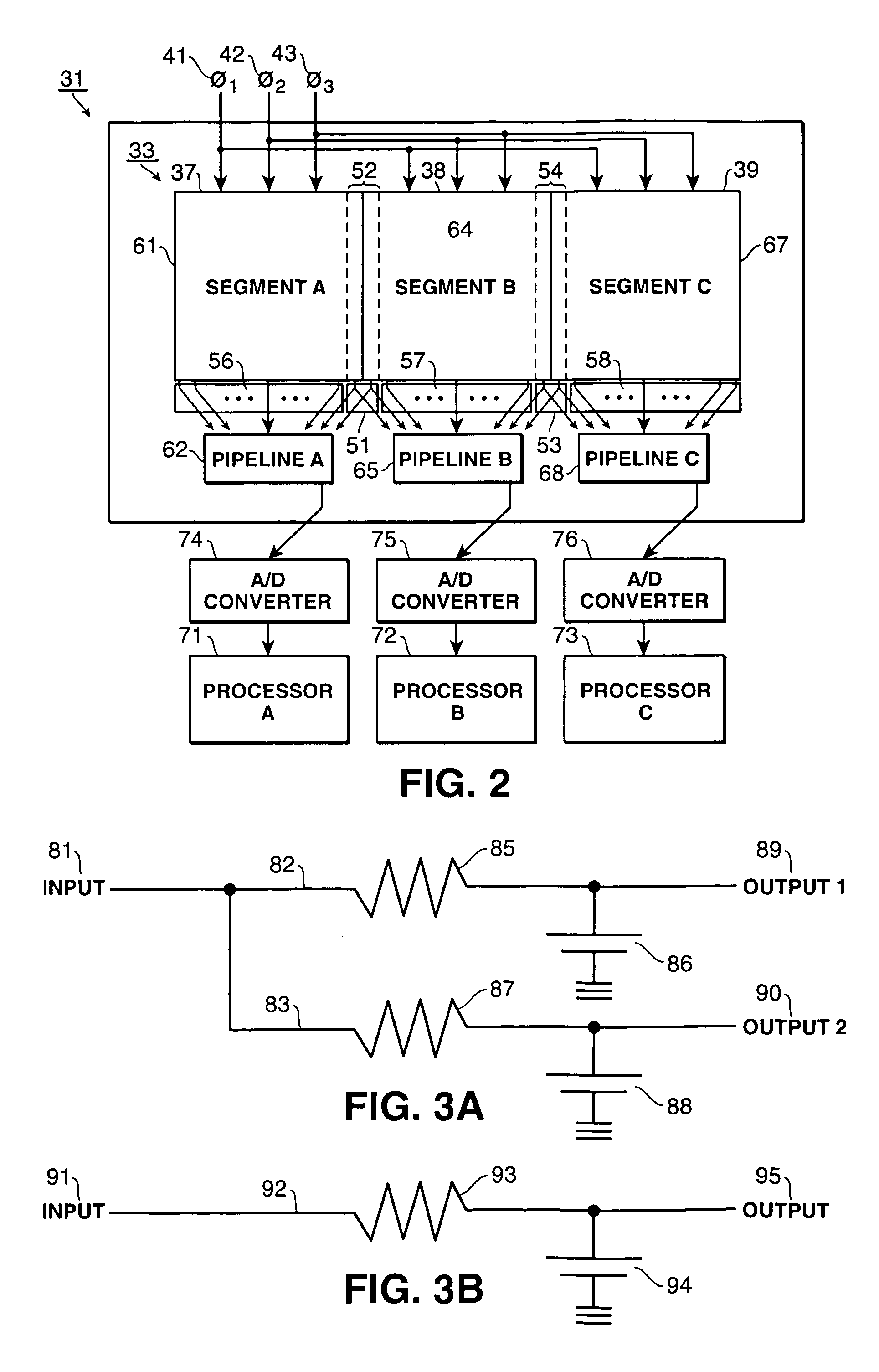
[0038]In more detail, FIG. 2 shows electronic imaging sensor chip 31 having sensor array 33, which includes mutually disjoint sensor segments A, B and C, designated at numerals 37, 38 and 39. Each of these sensor segments outputs rows of ch...
second embodiment
[0052]FIG. 5 is a representational view of a second embodiment of an electronic imaging sensor according to the invention.
[0053]Briefly, according to the second embodiment, an electronic imaging sensor includes a sensor array segmented into plural mutually disjoint segments, a respective plurality of output pipelines, each of which corresponds to each of the plural segments of the sensor array, and a respective plurality of processors. Each processor is coupled to a respective one of the output pipelines. The electronic imaging sensor also includes an output pipeline, or shift out line, for outputting pixel values of pixels in the overlap region to an intermediate buffer. The intermediate buffer provides duplicate pixel values to each processor whose segment borders the overlap region.
[0054]In more detail, FIG. 5 shows electronic imaging sensor chip 101 having sensor array 103, which includes sensor segment A 107, sensor segment B 108 and sensor segment C 109. Each of these sensor s...
third embodiment
[0066]FIG. 7 is a representational view of a third embodiment of an electronic imaging sensor according to the invention.
[0067]Briefly, according to the third embodiment, an electronic imaging sensor includes a sensor array segmented into plural mutually disjoint segments, a respective plurality of output pipelines, each of which corresponds to each of the plural segments of the sensor array, and a respective plurality of processors. Each processor is coupled to a respective one of the output pipelines. A communication link is provided between processors that border an overlap region, and duplicate pixels are communicated between the processors over the communication link.
[0068]In more detail, FIG. 7 shows electronic imaging sensor chip 141 having sensor array 143, which includes sensor segment A 147, sensor segment B 148 and sensor segment C 149. Each of these sensor segments outputs rows of charges or voltages for an image focused thereon in accordance with phased clocks φ1 151, φ...
PUM
 Abstract
Description
Claims
Application Information
 - R&D
- Intellectual Property
- Life Sciences
- Materials
- Tech Scout
- Unparalleled Data Quality
- Higher Quality Content
- 60% Fewer Hallucinations
Browse by: Latest US Patents, China's latest patents, Technical Efficacy Thesaurus, Application Domain, Technology Topic, Popular Technical Reports.
© 2025 PatSnap. All rights reserved.Legal|Privacy policy|Modern Slavery Act Transparency Statement|Sitemap|About US| Contact US: help@patsnap.com