Dual charge transport layer and photoconductive imaging member including the same

a charge transport layer and photoconductive imaging technology, applied in the direction of instruments, electrographic process apparatus, corona discharge, etc., can solve the problems of poor charge acceptance and cyclic instability, photoreceptor degradation, and charge transport molecules are frequently exposed to deleterious environmental conditions

Active Publication Date: 2006-03-28
XEROX CORP
View PDF19 Cites 58 Cited by
  • Summary
  • Abstract
  • Description
  • Claims
  • Application Information

AI Technical Summary

Benefits of technology

[0015]It is, therefore, an object of the present invention to provide an improved process for fabricating a photoconductive imaging member.
[0016]It is another object of the present invention to provide for an improved process for achieving greater stability of the electrographic imaging systems.
[0019]The imaging member prepared according to the present invention may be employed in any suitable and conventional electrophotographic imaging process which utilizes uniform charging prior to image wise exposure to activating electromagnetic radiation. Due to the inclusion of an oxidative inhibitor in the top layer of the charge transport layer, the imaging member of the invention exhibits improved xerographic performance (e.g. cyclic stability and charge uniformity) and a lengthening of the life of the photoconductive imaging member.

Problems solved by technology

In copiers, duplicators and electronic printers, such charge transport molecules are frequently exposed to deleterious environmental conditions induced by light, charging devices (such as corotrons, dicorotrons, scorotrons and the like), electric fields, oxygen, oxidants and moisture.
These unwanted chemical reactions can cause photoreceptor degradation, poor charge acceptance and cyclic instability.
The oxidative intermediates and their products usually degrade the surface of the photoreceptor and lead to various problems.
If the surface of the photoreceptor degrades as a result of chemical and photochemical reactions, the photoreceptor surface becomes conductive (e.g. electrical charges develop and can laterally migrate) and exhibits image quality degradation Depending on the degree of damage, the photoreceptor degradation can lead to poor image quality, or even an inability of a copier or an electronic printer to produce a print.
However, when the charge transport layer comprises a film forming resin and one or more of certain aromatic amines, diamines and hydrazone compounds, difficulties have been encountered with these photosensitive members when they are used under certain conditions in copiers, duplicators and printers.

Method used


Image

  • Dual charge transport layer and photoconductive imaging member including the same
  • Dual charge transport layer and photoconductive imaging member including the same
  • Dual charge transport layer and photoconductive imaging member including the same

Examples


example 1

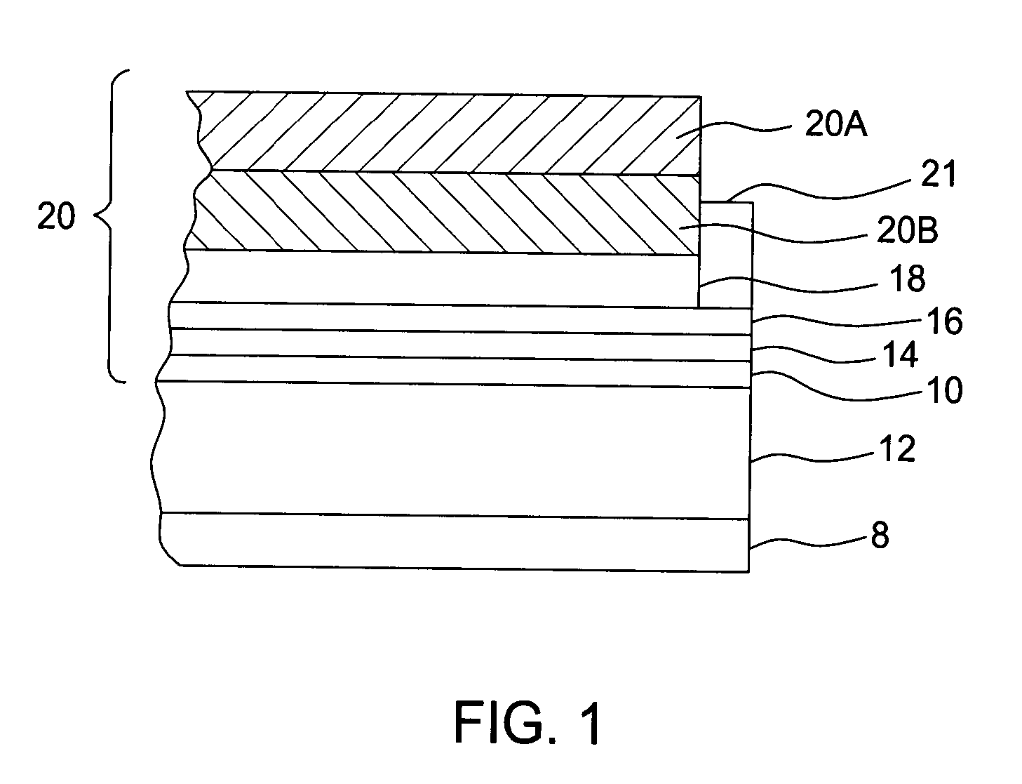
[0081]An imaging member was prepared by providing a 0.02 micrometer thick titanium layer coated on a biaxially oriented polyethylene naphthalate substrate (KALEDEX™ 2000) having a thickness of 3.5 mils, and applying thereon, with a gravure applicator, a solution containing 50 grams 3-amino-propyltriethoxysilane, 41.2 grams water, 15 grams acetic acid, 684.8 grams of 200 proof denatured alcohol and 200 grams heptane. This layer was then dried for about 5 minutes at 135° C. in the forced air drier of the coater. The resulting blocking layer (14) had a dry thickness of 500 Angstroms.

[0082]An adhesive layer (16) was then prepared by applying a wet coating over the blocking layer, using a gravure applicator, containing 0.2 percent by weight based on the total weight of the solution of copolyester adhesive (Ardel D100 available from Toyota Hsutsu Inc.) in a 60:30:10 volume ratio mixture of tetrahydrofuran / monochlorobenzene / methylene chloride. The adhesive layer was then dried for about 5 ...

example 2

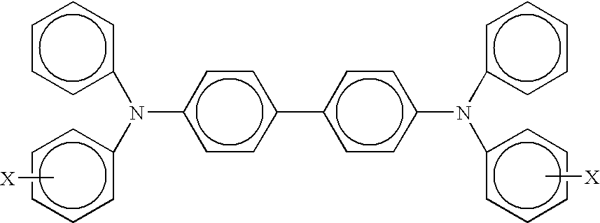
[0088]An imaging member was prepared as in Example 1 except each of the top and bottom layers of the charge transport layer contained 6.8% Irganox 1010® by weight of the dry solids. The weight ratio of 1:1 N,N′-diphenyl-N,N′-bis(3-methylphenyl)-1,1′-biphenyl-4,4′-diamine and Makrolon 5705® remained the same.

example 3

[0089]An imaging member was prepared as in Example 1 except the top layer of the charge transport layer contained 6.8% Irganox I-1010® by weight of the dry solids. The weight ratio of 1:1 N,N′-diphenyl-N,N′-bis(3-methylphenyl)-1,1′-biphenyl-4,4′-diamine and Makrolon 5705® remained the same.


PUM


Abstract

A photoconductive imaging member is disclosed comprising a charge generation layer and a charge transport layer comprising an oxidative inhibitor. An electrophotographic imaging process using the imaging member of the invention is also described.

Description

FIELD OF THE INVENTION[0001]The present invention is directed to a dual charge transport layer comprising a top layer adjacent to a bottom layer. The top layer comprises an oxidative inhibitor. The bottom layer which is adjacent to a charge generation layer on a substrate provides a barrier for the diffusion of the oxidative inhibitor to the charge generation layer between the top layer and the charge generation layer. The invention is also directed to photoconductive imaging members comprising such charge transport layer.BACKGROUND OF THE INVENTION[0002]This invention relates in general to a process for fabricating a photoconductive imaging member, and more specifically to the formation of a dual charge transport layer.[0003]In the art of electrophotography, a photoconductive imaging member containing a photoconductive layer is imaged by first uniformly electrostatically charging the imaging surface of the imaging member. The member is then exposed to a pattern of activating electr...

Claims


Application Information

Patent Timeline
Patent Type & Authority Patents(United States)
IPC IPC(8): G03G5/047G03G5/043G03G5/05G03G5/06
CPCG03G5/047G03G5/06G03G5/05
Inventor PAI, DAMODAR M.EVANS, KENT J.CARMICHAEL, KATHLEEN M.HELBIG, COLLEEN A.YANUS, JOHN F.TONG, YUHUAFULLER, TIMOTHY J.GARLAND, KAREN S.DEFEO, PAUL J.LYNCH, ANITA P.
Owner XEROX CORP
Why Eureka
Try Eureka