Method and system for manufacturing electronic device, electronic device, and electro-optical apparatus

a technology of electronic devices and electrooptical devices, applied in the direction of identification means, instruments, electric programme control, etc., can solve the problems of difficult to use environmental load data, inability to maintain collected environmental load data, and the most important issue of ‘energy saving’

Active Publication Date: 2008-03-18
BOE TECH GRP CO LTD
View PDF4 Cites 221 Cited by
  • Summary
  • Abstract
  • Description
  • Claims
  • Application Information

AI Technical Summary

Benefits of technology

[0013]An advantage of some aspects of the invention is that it provides a method and system for manufacturing an electronic device, an electronic device, and an electro-optical apparatus, which can collect the environmental load data for each product.
[0020](4) It is possible to compare the environmental information between different regions. For example, when the same device is employed both factories installed in Japan and another country, it is possible to collect in units of products the environmental load data of each product in each factory. Accordingly, it is possible to analyze problems caused by a regional difference, thereby improving the process and reducing the environmental load.
[0028]According to the aspect, it is possible to transmit the number of work pieces, which is counted by the counter, the environmental information and processing time, which are measured in units of lots, to the work information management unit corresponding to each lot, and store them in the work information management unit. Accordingly, it is possible to manage the environmental load data for each lot. In addition, since the processing unit transmits the environmental information together with the lot identification number, the work information management unit can determine whether or not the lot identification number is identical to the assigned lot identification number. Accordingly, it is possible to make a communication only between the lot and the work information management unit, thereby avoiding making a false transmission.
[0038]According to the method of manufacturing the electronic device, it is possible to optimize manufacturing process management, thereby efficiently manufacturing the electro-optical apparatus. In addition, according to the electronic device and the electro-optical apparatus of the invention, it is possible to optimize manufacturing process management, thereby efficiently manufacturing the electronic device and the electro-optical apparatus.

Problems solved by technology

Among them, ‘energy saving’ is becoming the most important issue.
However, the following problems are present in methods disclosed in JP-A-1993-309552:(1) In the above method, it is possible to identify and manage individual products.
However, there is a problem in that it is not possible to maintain collected environmental load data in the case of collecting the environmental load data according to each product in a processing apparatus.(2) Barcodes attached to the individual products may be detached from the products when the products are processed under a high-temperature environment in a process of manufacturing an electronic device.
Accordingly, it is difficult to use the environmental load data after measuring the environmental load data for each product in each processing apparatus and saving the measured environmental load data for later use.

Method used


Image

  • Method and system for manufacturing electronic device, electronic device, and electro-optical apparatus
  • Method and system for manufacturing electronic device, electronic device, and electro-optical apparatus
  • Method and system for manufacturing electronic device, electronic device, and electro-optical apparatus

Examples


Embodiment Construction

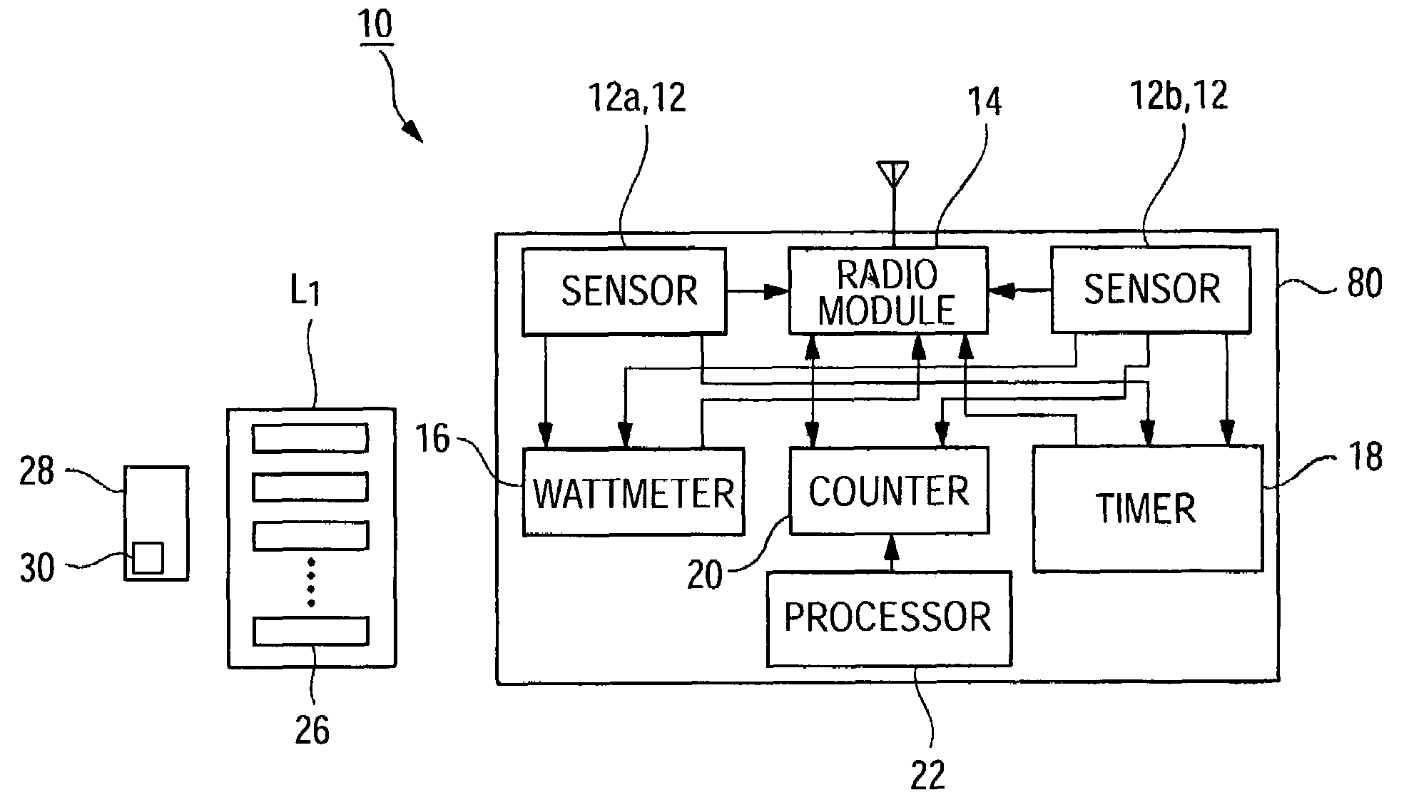
[0053]Hereinafter, embodiments of the invention will be described with reference to the accompanying drawings.

[0054]The invention describes a system for manufacturing a thin film diode (TFD) element (a system for manufacturing an electronic device) which collects data concerning environmental load, for example, upon manufacturing a TFD element that is used in a liquid crystal display device. Also, even though an actual TFD element is manufactured by performing a predetermined process using a plurality of processing devices, the present embodiment, for easy understanding of the invention, only describes a system for manufacturing the TFD element in which a single processing device (etching device) is used. Also, even though plural substrates of lots are carried into each processing device in the system for manufacturing the TFD element, the present embodiment only describes a case where a single substrate of the lot is carried into the processing device. Also, in the accompanying dra...


PUM

PropertyMeasurementUnit
frequencyaaaaaaaaaa
frequencyaaaaaaaaaa
timeaaaaaaaaaa

Abstract

A system for manufacturing an electronic device having a processing unit which includes a timer that processes a plurality of lots each having a plurality of work pieces and measuring in units of lots a processing time of the work pieces constituting the respective lots, an environmental information measurement module that measures environmental information corresponding to the processing time of the work pieces measured in units of lots, and a communication module for transmission and reception, and a work information management unit having a storage module which is provided to correspond to each lot, communicates with the communication module of the processing unit, and receives and stores the processing time and the environmental information of the work pieces of the lot.

Description

BACKGROUND[0001]1. Technical Field[0002]The present invention relates to a method and system for manufacturing an electronic device, to an electronic device, and to an electro-optical apparatus.[0003]2. Related Art[0004]Recently, effects on the environment due to the manufacture of products have been of increasing concern. In order to achieve harmony with the environment, for example, ‘Energy saving’, ‘Resource saving’, and ‘Waste reduction’ have to be achieved. ‘Energy saving’ implies, for example, reduction in power consumption. ‘Resource saving’ implies, for example, reduction in paper consumption. ‘Waste reduction’ implies, for example, paper recycling. Among them, ‘energy saving’ is becoming the most important issue.[0005]In order to achieve ‘energy saving’, environmental load data, such as power consumption per product, needs to be collected upon manufacturing or supplying products. Accordingly, it is possible to achieve ‘energy saving’ by determining the power consumption per...

Claims


Application Information

Patent Timeline
Patent Type & Authority Patents(United States)
IPC IPC(8): G06F19/00G02F1/13G05B19/418G09F9/00
CPCG06Q10/04G05B19/418
Inventor UCHIYAMA, KENJI
Owner BOE TECH GRP CO LTD
Why Eureka
Try Eureka