Isolation device over field in a memory device

a memory device and isolation device technology, applied in the field of memory devices, can solve the problems of reducing the retention time of memory cells, affecting the operation of memory devices, so as to improve the refresh operation, improve isolation, and reduce the effect of charge leakag

Inactive Publication Date: 2006-03-28
MICRON TECH INC
View PDF23 Cites 20 Cited by
  • Summary
  • Abstract
  • Description
  • Claims
  • Application Information

AI Technical Summary

Benefits of technology

[0008]The present invention provides structures and methods for improving isolation between adjacent memory cells to reduce the charge leakage, to improve the refresh operation, increase the time availability of the data, and offer alternative ways for replacing defected memory cells.

Problems solved by technology

This leakage reduces the retention time of the memory cell and may create invalid data.
In some cases, these isolation techniques provide inadequate isolation.
Increasing the number of refresh cycles wastes power and reduces the time that the valid data is available.
This double-row redundancy method is used because the isolation devices in these memory devices may not provide enough insolation between adjacent rows.

Method used


Image

  • Isolation device over field in a memory device
  • Isolation device over field in a memory device
  • Isolation device over field in a memory device

Examples


Embodiment Construction

[0022]The following description and the drawings illustrate specific embodiments of the invention sufficiently to enable those skilled in the art to practice it. Other embodiments may incorporate structural, logical, electrical, process, and other changes. In the drawings, like numerals describe substantially similar components throughout the several views. Examples merely typify possible variations. Portions and features of some embodiments may be included in or substituted for those of others. The scope of the invention encompasses the full ambit of the claims and all available equivalents.

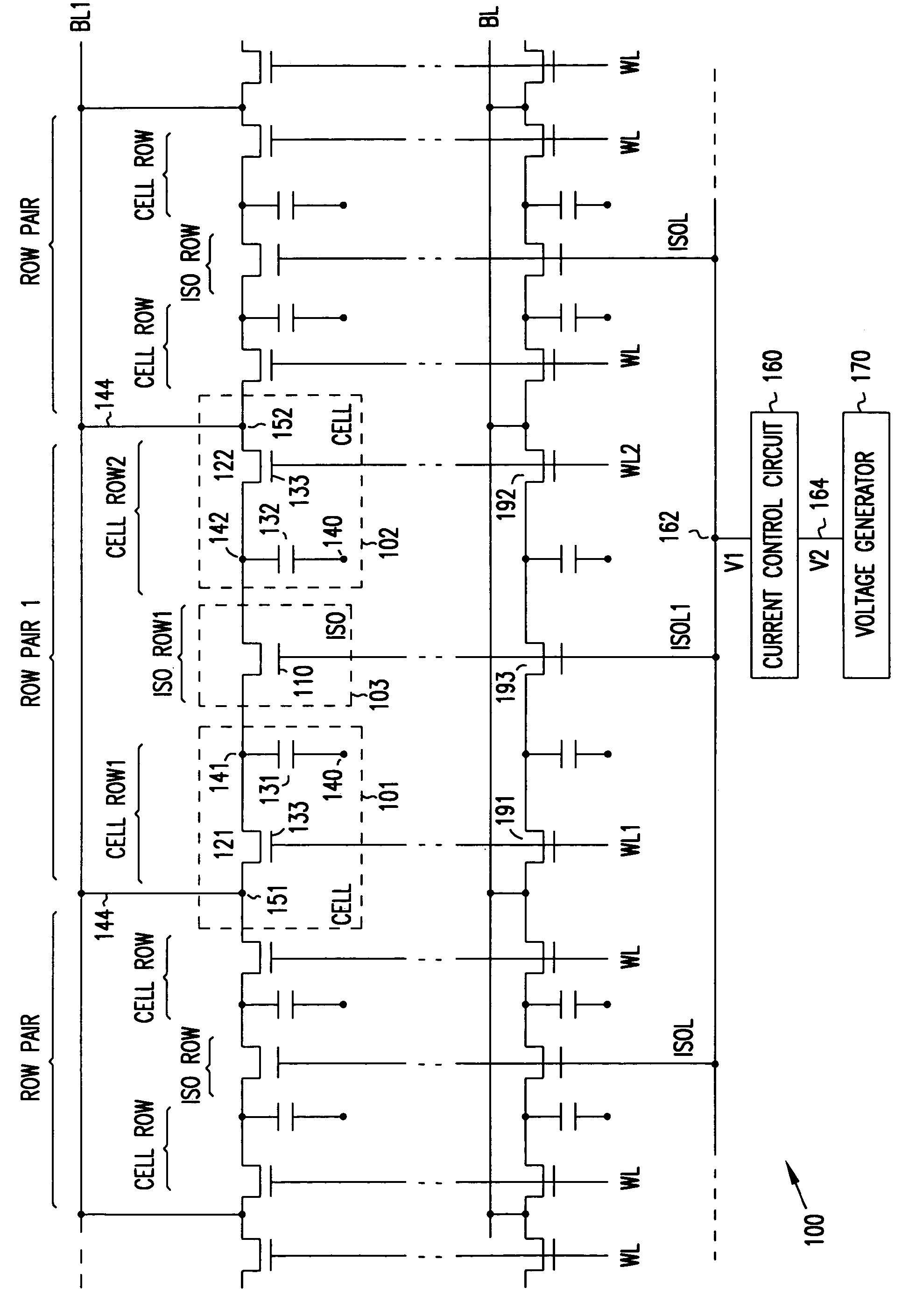
[0023]FIG. 1 is a schematic diagram of a memory array according to an embodiment of the invention. Memory array 100 includes many memory cells (CELL) arranged in rows (CELL ROW) and columns (CELL COL), the rows being arranged in row pairs (ROW PAIR) with each including a first cell row (CELL ROW1) and a second cell row (CELL ROW2). For simplicity, FIG. 1 shows only three row pairs and two cell c...


PUM


Abstract

A memory device includes isolation devices located between memory cells. A plurality of isolation lines connects the isolation devices to a positive voltage during normal operations but still keeps the isolation devices in the off state to provide isolation between the memory cells. A current control circuit is placed between the isolation lines and a power node for reducing a current flowing between the isolation lines and the power node in case a deflect occurs at any one of isolation devices.

Description

[0001]This application is a Continuation of U.S. application Ser. No. 10 / 233,325, filed Aug. 29, 2002, now U.S. Pat. No. 6,834,019, which is incorporated herein by reference.FIELD[0002]The present invention relates generally to semiconductor devices, and in particular to memory devices.BACKGROUND[0003]Memory devices reside in computers and many electronic products to store data. A typical memory device has many memory cells, each holding a charge that represents a value of a bit of data.[0004]Some memory devices hold the charge in a capacitor of each memory cell. The charge in the capacitor leaks overtime. Therefore, some of these memory devices have refresh cycles to frequently refresh the charge to maintain its original value to keep the data valid.[0005]In some memory devices, the charge in the capacitor of one memory cell leaks to the substrate or to an adjacent capacitor of another memory cell. This leakage reduces the retention time of the memory cell and may create invalid da...

Claims


Application Information

Patent Timeline
Patent Type & Authority Patents(United States)
IPC IPC(8): G11C7/00G11C7/12G11C7/18G11C11/4097
CPCG11C7/02G11C7/12G11C7/18G11C11/4097G11C11/401Y10S257/906G11C29/816G11C2207/002G11C2207/005
Inventor TRAN, LUAN C.PORTER, STEPHEN R.GRAHAM, SCOT M.HOWELL, STEVEN E.
Owner MICRON TECH INC
Why Eureka
Try Eureka