Multi-package stack module
a stack module and multi-package technology, applied in the field of electronic modules, can solve the problems of limited input/output terminal area, and the limitations of enhancing the density of chip integration
- Summary
- Abstract
- Description
- Claims
- Application Information
AI Technical Summary
Problems solved by technology
Method used
Image

Examples
first embodiment
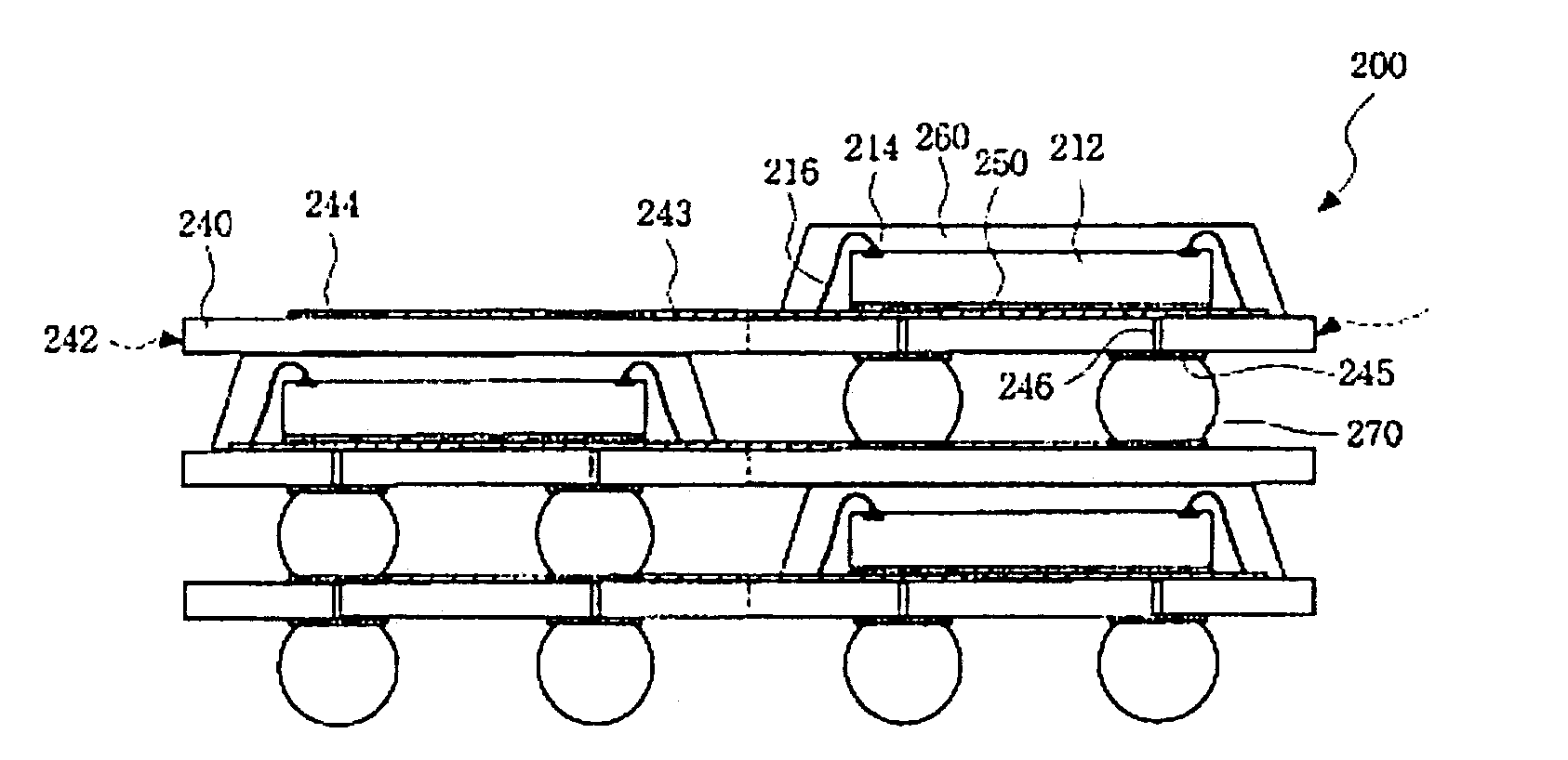
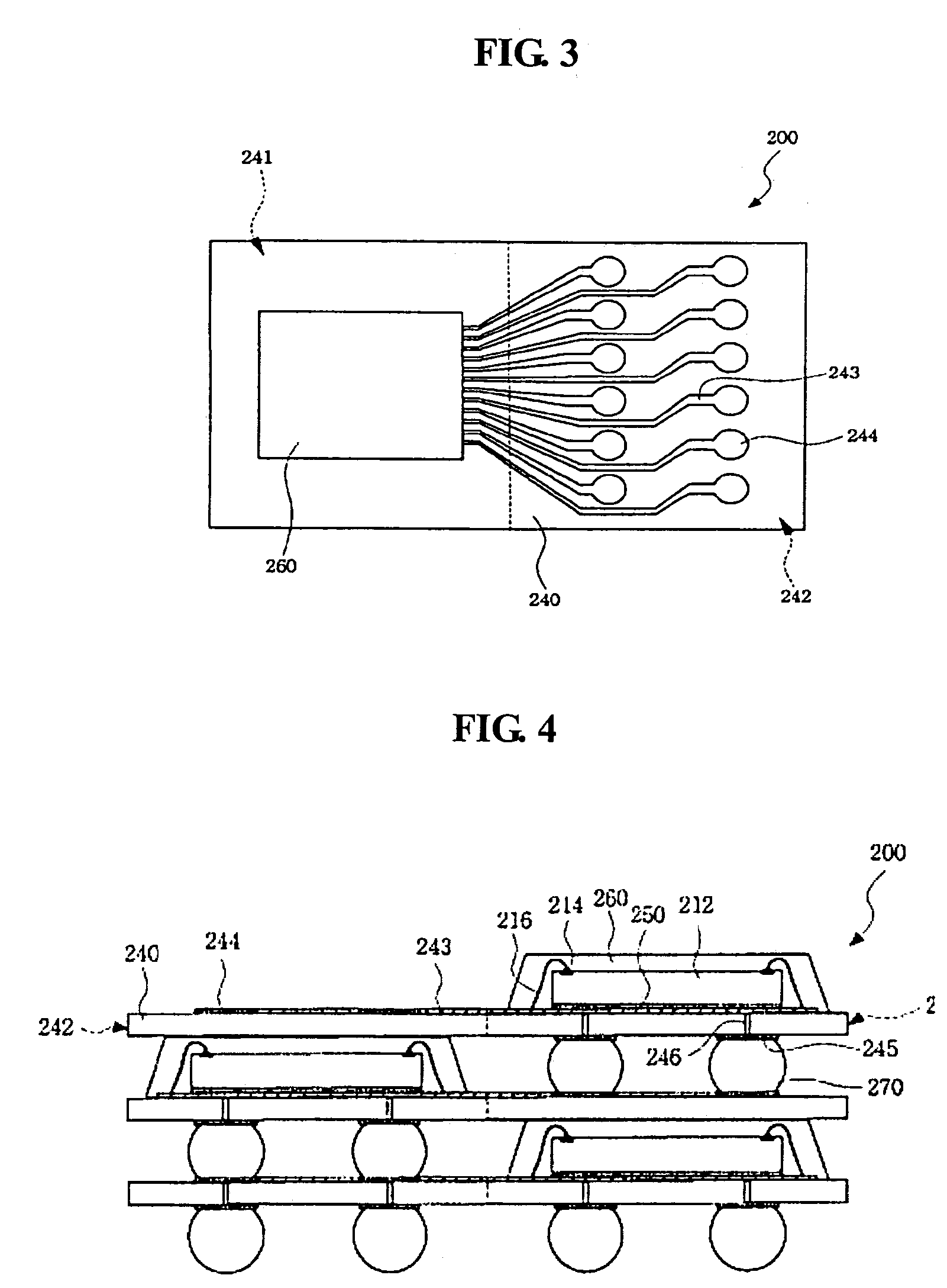
[0028]A multi-package module (200) according to the present invention will be described referring to FIG. 4. As shown in FIG. 4, packages such as those described in the FIG. 3 are stacked in a manner such that chips (212) of the stacked packages are not in vertical alignment with each other. In other words, the chips (212) of the stacked packages are laterally offset from each other. Preferably, the chips (212) do not overlap with each other. The solder bumps (270) of the upper package are electrically connected to the first bump pads (244) formed on the bump pad area (242) of the lower adjacent package. Because the solder bumps (270) are formed on the second side of the board (240) in a space corresponding to the chip installation area (241), the chip installation area (241) of the upper package becomes positioned above the bump pad area (242) of the lower packages. Therefore, the chip installation area (241) of the two adjacent stacked packages are not in vertical alignment with e...
second embodiment
[0029]FIG. 5 is a sectional view of a multi-package module (300) according to the present invention. The basic structure of the multi-package module (300) is the same as that of the multi-package module (200) except for an additional electronic device (380) disposed on the bump pad area (342) of the highest package of the multi-package module (300).
[0030]The electronic device (380) may be a capacitor, an inductor, a resistor, or other electronic elements. Although one electronic device (380) is described in FIG. 5, a plurality of electronic devices can be disposed on the bump pad area (342). Preferably, the electronic device (380) is electrically connected to the first bump pad (344).
third embodiment
[0031]FIG. 6 is a sectional view of a multi-package module (400) according to the present invention. The basic structure of the multi-package module (400) is the same as that of the multi-package module (200) except that at least one package is a multi-chip package. As shown in FIG. 6, at least two chips (412, 422) are stacked in a package and the two chips (412, 422) are electrically connected to redistribution patterns (443) by bonding wires (416, 426) and to bump pads (444, 445) by redistribution patterns (443). The number of chips employed can be determined according to their usage.
[0032]The multi-package module structure described in the specification can also be adapted to the system-in module including a memory, central processing units (CPUs), and other electronic devices in a single module.
[0033]Because of the configuration of the multi-package module described in the embodiments of FIGS. 3–6, it is possible to prevent chips in one location in a stacked package from being a...
PUM
 Abstract
Description
Claims
Application Information
 - R&D
- Intellectual Property
- Life Sciences
- Materials
- Tech Scout
- Unparalleled Data Quality
- Higher Quality Content
- 60% Fewer Hallucinations
Browse by: Latest US Patents, China's latest patents, Technical Efficacy Thesaurus, Application Domain, Technology Topic, Popular Technical Reports.
© 2025 PatSnap. All rights reserved.Legal|Privacy policy|Modern Slavery Act Transparency Statement|Sitemap|About US| Contact US: help@patsnap.com