Magnetically actuated microelectrochemical systems actuator

a microelectrochemical and actuator technology, applied in the direction of snap-action arrangement, magnetism bodies, instruments, etc., can solve the problems of physical connection and electrically conductive layers, and achieve the effects of reducing the number of coils, and preventing cross-talk and excessive and possibly damaging curren

Inactive Publication Date: 2006-06-20
MICROSOFT TECH LICENSING LLC
View PDF77 Cites 13 Cited by
  • Summary
  • Abstract
  • Description
  • Claims
  • Application Information

AI Technical Summary

Benefits of technology

[0013]A limitation of the MUMPs fabrication process is that layers that are physically connected are also electrically conductive. And, in the preferred embodiments, the actuator coils, the bridge, and the mirror are physically coupled and thus electrically conductive. Accordingly, symmetric bipolar current is applied to the coil pairs to maintain the mirror at zero volts and prevent cross-talk and excessive and possibly damaging current between the coils.
[0014]The actuator of the present invention is fabricated in conformal layers as described below in connection with the MUMPs process. Accordingly, the actuators, bridges, and mirror are formed as layers that are close to one another. Therefore, in order to provide a desired range of motion, a steady-state elevating current is applied to the actuators that creates a substantially similar magnetic field in each actuator to extend each actuator a similar amount and raise the mirror above (i.e., away from) the substrate on which the components are formed. The mirror may then be moved by providing a modulation current to individual actuators that increases or decreases the magnetic field strength in those particular actuators, to raise or lower one corner, or side, of the mirror relative to the other mirror portions. In this manner, a mirror may be tilted to control a path of a light beam to form a portion of a video image. Alternatively, actuators of the present invention fabricated by means other than MUMPs, may provide for electrical separation between the coils and the mirror and thereby simplify the arrangement of coils in the actuator.
[0026]After the ANCHOR1 etch, a first structural layer of polysilicon (POLY 1) 114 is deposited at a thickness of 2.0 μm. A thin 200 nm PSG layer 116 is deposited over the POLY 1 layer 114 and the wafer is annealed at 1050° C. for 1 hour (FIG. 7). The anneal dopes the POLY 1 layer with phosphorus from the PSG layers both above and below it. The anneal also serves to significantly reduce the net stress in the POLY 1 layer. The POLY 1 and PSG masking layers are lithographically patterned using a mask designed to form the structure of the POLY1 layer. The PSG layer is etched to produce a hard mask for the subsequent polysilicon etch. This hard mask is more resistant to the polysilicon etch chemistry than the photoresist and ensures a better transfer of the pattern into the POLY 1 layer. After etching the POLY 1 layer (FIG. 8), the photoresist is stripped and the remaining oxide hard mask is removed by RIE.
[0029]Second, an ANCHOR2 etch (depicted at 122) is provided to etch both the First and Second Oxide layers 108, 118 in one step to eliminate misalignment that can occur between separately etched holes. More importantly, the ANCHOR2 etch eliminates the need to make a cut in the First Oxide layer that is unrelated to anchoring a POLY 1 structure, which would needlessly expose the substrate to subsequent processing that can damage either the POLY 0 or Nitride layers. For the ANCHOR2 etch, the Second Oxide layer is lithographically patterned and etched by RIE in the same way as the POLY1_POLY2_VIA etch. FIG. 11 shows the wafer cross section after both POLY1_POLY2_VIA and ANCHOR2 etches have been completed.

Problems solved by technology

A limitation of the MUMPs fabrication process is that layers that are physically connected are also electrically conductive.

Method used


Image

  • Magnetically actuated microelectrochemical systems actuator
  • Magnetically actuated microelectrochemical systems actuator
  • Magnetically actuated microelectrochemical systems actuator

Examples


Embodiment Construction

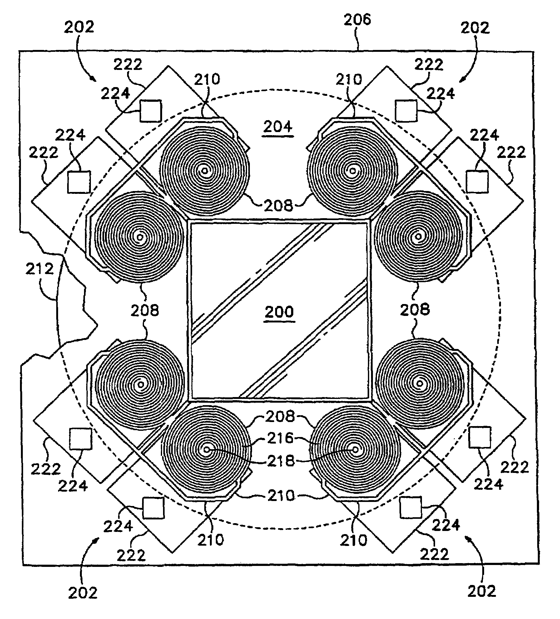
[0040]A preferred embodiment of the present invention is described below with reference to the accompanying FIGS. 16–20. The present invention provides an electrically controlled actuator. While the present actuator is shown controlling a mirror surface—a common application of microelectrical mechanical actuators—the actuator may be used to control other physical structures, such as lenses, valves, and switches.

[0041]In the present invention, a repulsive magnetic force is used to elevate and control an orientation of the mirror, or other object. In a first preferred embodiment, electrical input is provided to expandable, semiconductor coils to create a variable magnetic field. A permanent magnet located near the semiconductor coils provides an opposing fixed magnetic force that causes the semiconductor coils to expand in a predictable and controllable manner. This coil expansion provides mechanical motion that can move an object such as the exemplary mirror. The electrical input may...


PUM

PropertyMeasurementUnit
depthaaaaaaaaaa
thicknessaaaaaaaaaa
thickaaaaaaaaaa

Abstract

A microelectrical mechanical system (MEMS) actuator having electrically conductive coils that create first magnetic fields that are opposed by a second magnetic field is disclosed. The actuator includes two coils having dual, interspersed Archimedean spirals. Within an actuator, one coil is arranged with spirals that proceed clockwise, while the other coil is provided with spirals that proceed counterclockwise. An electrically conductive bridge mechanically couples the two coils of each actuator to a mirror. Opposing magnetic fields are created to provide a force that urges the coils to expand so that the outermost portions of the coil extend upward, away from the substrate, and lift the bridge and mirror. Control current may then be modulated to increase and decrease the coil's magnetic field strength thereby increasing and decreasing the coil's extension to raise and lower relative to the substrate.

Description

BACKGROUND OF THE INVENTION[0001]1. Field of the Invention[0002]This invention pertains to electrically controlled actuators and more particularly pertains to microelectromechanical systems (MEMS) actuators.[0003]2. Description of the Related Art[0004]Electrically controlled actuators receive electrical signal input and provide a mechanical output that can be used to move objects. The electrical signal can control the mechanical output to control a rate and amount of movement applied to the object. Large, electrically controlled actuators are common in mechanical systems to control valves, pumps, and move objects.[0005]Recent innovations require control of very small components. In U.S. Pat. No. 5,808,384 a photolithographic process is used to fabricate a micromechanical actuator to control switches, relays, and valves. However, the invention of the U.S. Pat. No. 5,808,384 does not teach a means to move objects toward and away from the plane of the substrate upon which the device is...

Claims


Application Information

Patent Timeline
Patent Type & Authority Patents(United States)
IPC IPC(8): G02B26/08B81B3/00B81B5/00G02B6/35H01F7/08H01F7/14H01H50/00
CPCB81B3/0021G02B6/3572G02B26/085H01F7/08H01F7/14H01H50/005H02K41/0356Y10S359/904B81B2203/058G02B6/3518G02B6/358G02B6/3584H01F7/066H01F21/04H01F2005/006H01F2007/068B81B2201/042G02B26/101
Inventor LEVITAN, JEREMY A.SINCLAIR, MICHAEL J.
Owner MICROSOFT TECH LICENSING LLC
Why Eureka
Try Eureka