Double gate device having a heterojunction source/drain and strained channel

a heterojunction source/drain and channel technology, applied in the field of semiconductor devices having very small dimensions, can solve the problems of uneven device uniformity within the circuit, different scaling challenges, and inability to adequately control the implant structure with conventional semiconductor fabrication equipment,

Active Publication Date: 2006-06-27
NXP USA INC
View PDF5 Cites 39 Cited by
  • Summary
  • Abstract
  • Description
  • Claims
  • Application Information

AI Technical Summary

Problems solved by technology

However, different challenges have been encountered in the scaling of transistor structures much below 100 nm.
Additionally, when transistor dimensions on the order of 100 nm and smaller are used, implants cannot be adequately controlled with conventional semiconductor fabrication equipment.
Channel dopant fluctuations adversely affect device uniformity within circuits.
However, channel doping is not an efficient method for ultra-thin devices due to the large amount of channel impurities that are required.
Therefore, highly doped ultra-thin devices are even more susceptible to threshold voltage fluctuations.
Additionally, high channel doping concentrations degrade both electron and hole mobility and promote source / gate and drain / gate junction leakage.
However, when thin-body devices are being implemented, the depth available for the stressor material is insufficient to adequately strain the channel.
Another issue with this technique is that the silicon material is recessed with an etch process.
Stopping the etch process at a desired depth is a challenge and subject to variation.
Additionally, re-growth of the stressor material on the remaining ultra-thin silicon is problematic.
Additionally, this method does not apply to the known FINFET structures or any thin-body transistor devices.
Therefore, another issue with this approach is that the presence of SiGe in the transistor's channel increases the transistor's off-state current leakage.
Additionally, this method does not apply to the known FINFET structures or any vertical thin body double gate transistor.

Method used


Image

  • Double gate device having a heterojunction source/drain and strained channel
  • Double gate device having a heterojunction source/drain and strained channel
  • Double gate device having a heterojunction source/drain and strained channel

Examples


Embodiment Construction

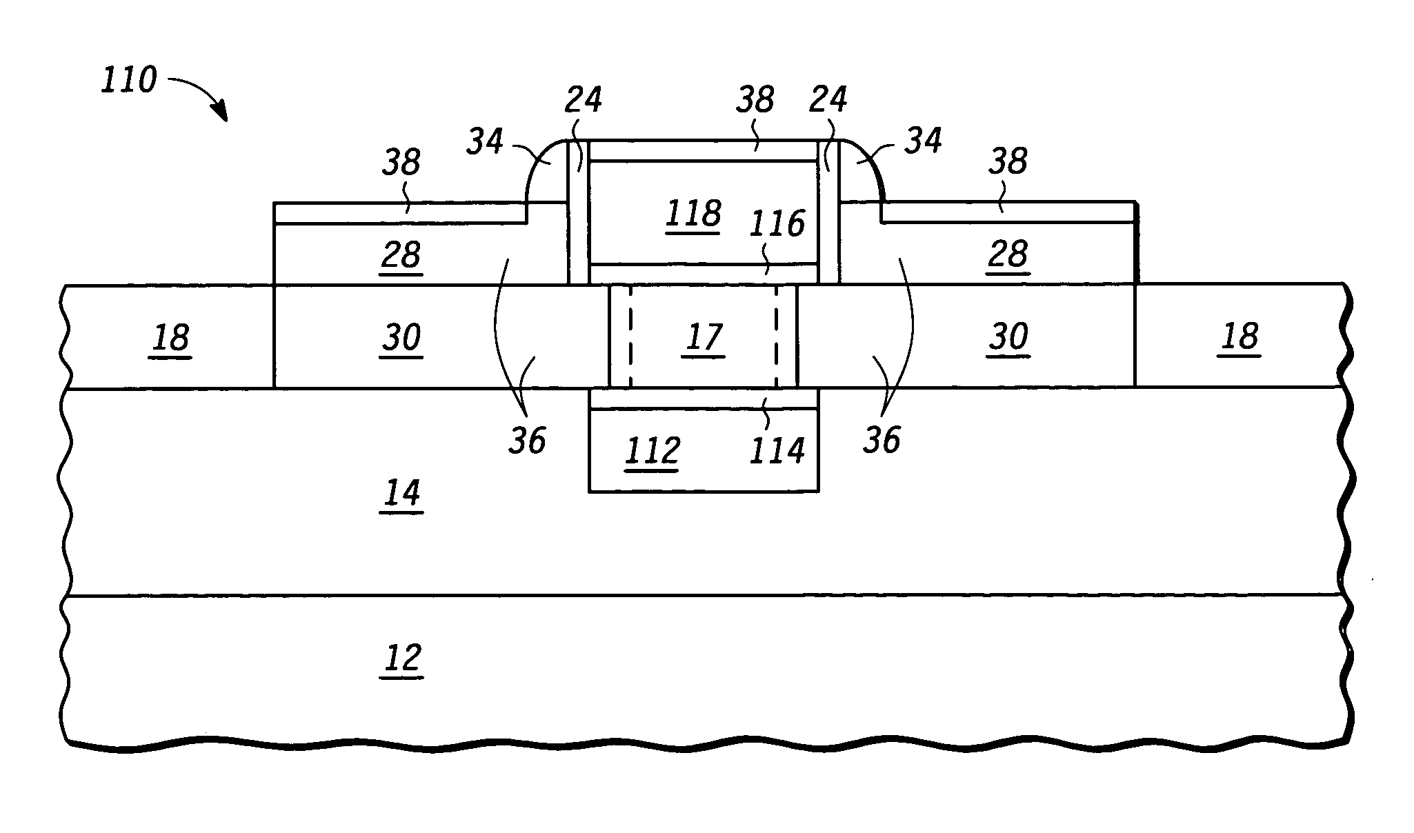
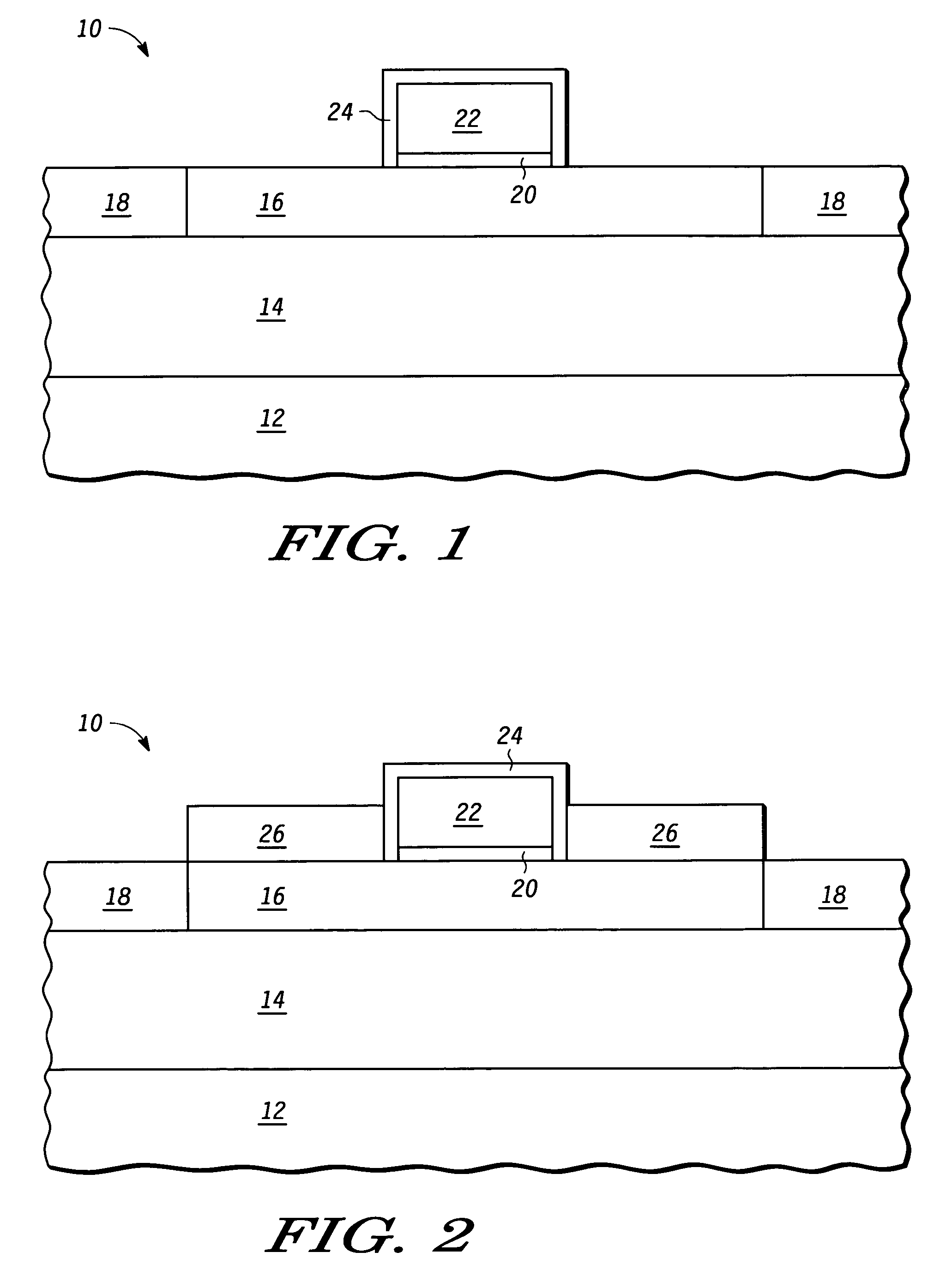
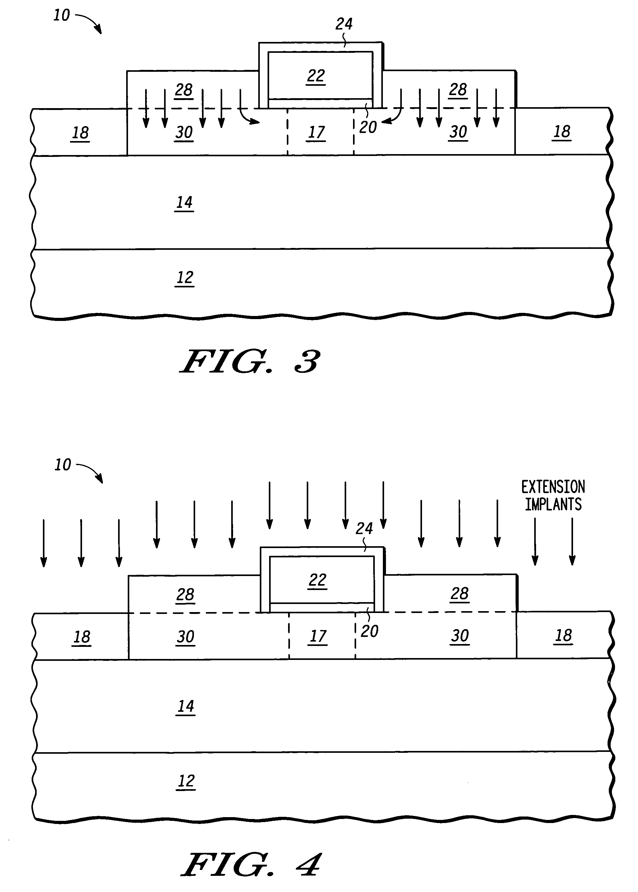
[0015]Illustrated in FIG. 1 is a semiconductor device 10 in accordance with the present invention. A substrate 12 is provided. In one form substrate 12 is silicon. However, any semiconductor material may be used. An overlying dielectric layer 14 is formed. Wafer bonding or implantation of an oxygen species material may be used to form the dielectric layer 14. In one form, the dielectric layer 14 is an oxide. A semiconductor layer 16 is formed and patterned overlying a portion of the dielectric layer 14. In one form the semiconductor layer 16 is silicon and has a thickness such that an aspect ratio that is equal to the gate length divided by the thickness of semiconductor layer 16 is at least three. Therefore, semiconductor layer 16 is relatively thin. Adjacent the semiconductor layer 16 is isolation region 18. It should be understood that isolation region 18 may either be a void of material or any dielectric material. Therefore, in one form the isolation region 18 is a void. A gate ...


PUM


Abstract

A semiconductor device (10) is formed by positioning a gate (22) overlying a semiconductor layer (16) of preferably silicon. A semiconductor material (26) of, for example only, SiGe or Ge, is formed adjacent the gate over the semiconductor layer and over source / drain regions. A thermal process diffuses the stressor material into the semiconductor layer. Lateral diffusion occurs to cause the formation of a strained channel (17) in which a stressor material layer (30) is immediately adjacent the strained channel. Extension implants create source and drain implants from a first portion of the stressor material layer. A second portion of the stressor material layer remains in the channel between the strained channel and the source and drain implants. A heterojunction is therefore formed in the strained channel. In another form, oxidation of the stressor material occurs rather than extension implants to form the strained channel.

Description

CROSS REFERENCE TO RELATED APPLICATION[0001]This application is related to our U.S. Patent Application, U.S. Ser. No. 10 / 954,121, now U.S. Pat. No. 7,018,901, entitled “Method For Forming A Semiconductor Device Having A Strained Channel And A Heterojunction Source / Drain”, filed simultaneously herewith and assigned to the assignee hereof.FIELD OF THE INVENTION[0002]This invention relates generally to semiconductor, and more specifically, to making semiconductor devices having very small dimensions.BACKGROUND OF THE INVENTION[0003]Semiconductor devices, such as transistor structures, continue to be scaled to smaller dimensions as process lithography improves. However, different challenges have been encountered in the scaling of transistor structures much below 100 nm. Additionally, when transistor dimensions on the order of 100 nm and smaller are used, implants cannot be adequately controlled with conventional semiconductor fabrication equipment. Channel dopant fluctuations adversel...

Claims


Application Information

Patent Timeline
Patent Type & Authority Patents(United States)
IPC IPC(8): H01L27/108
CPCH01L29/42392H01L29/66628H01L29/66742H01L29/78687H01L29/785H01L29/78621H01L29/78648H01L29/7842H01L21/18
Inventor THEAN, VOON-YEWSADAKA, MARIAM G.WHITE, TED R.BARR, ALEXANDER L.KOLAGUNTA, VENKAT R.NGUYEN, BICH-YENVARTANIAN, VICTOR H.ZHANG, DA
Owner NXP USA INC
Why Eureka
Try Eureka