Building metal pillars in a chip for structure support

a technology of structure support and metal pillars, which is applied in the direction of semiconductor devices, semiconductor/solid-state device details, electrical apparatus, etc., can solve the problems of increasing the tendency of stacked via-studs of present and future interconnection wiring schemes to crack, metal void formation and cracking within the interconnection,

Active Publication Date: 2006-06-27
GLOBALFOUNDRIES U S INC
View PDF9 Cites 43 Cited by
  • Summary
  • Abstract
  • Description
  • Claims
  • Application Information

AI Technical Summary

Benefits of technology

[0015]The present invention provides new semiconductor processes and integrated circuit (IC) structures which incorporate stacked via pillars in multilevel interconnection structures and wiring of semiconductor IC chips with high conductivity metallurgy and low-k dielectric materials, particularly with a high coefficient of thermal expansion and / or air gap bridging, to provide improved structural support and mechanical stability under large thermal excursions. The stacked via pillar structure support is designed for a post CMP (chemical / mechanical polishing) process when the air gaps are formed.

Problems solved by technology

This stress build up has resulted in line buckling and liner deformation in stacked vias (LSM, SRAM) that lead to metal void formation and cracking within the interconnect.
The continuing trend of dimensional shrinkage (smaller D) and increased wiring levels (larger H) in multilevel interconnections lead to much higher H to D ratios, thereby making the stacked via-studs of present and future interconnection wiring schemes increasingly more prone to cracks.
The crack propensity also increases with the range of temperature cycles and the number of cycles, showing that cracks are generated by metal fatigue, a phenomenon not been seen before in integrated circuit wiring.
The negligibly small compressive stress in low-k materials, along with the large thermal expansion mismatch between copper and low-k dielectric, e.g., SiLK, are root causes for the observed fatigue failure.
The prior art has undoubtedly provided solutions and methods for relieving mechanical stress, however the solutions and methods have generally had an adverse impact upon design flexibility that restricts the techniques that circuit designers can use to design chips.

Method used


Image

  • Building metal pillars in a chip for structure support
  • Building metal pillars in a chip for structure support
  • Building metal pillars in a chip for structure support

Examples


Embodiment Construction

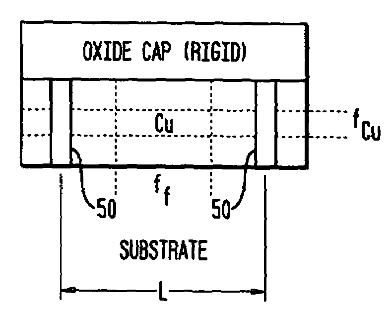
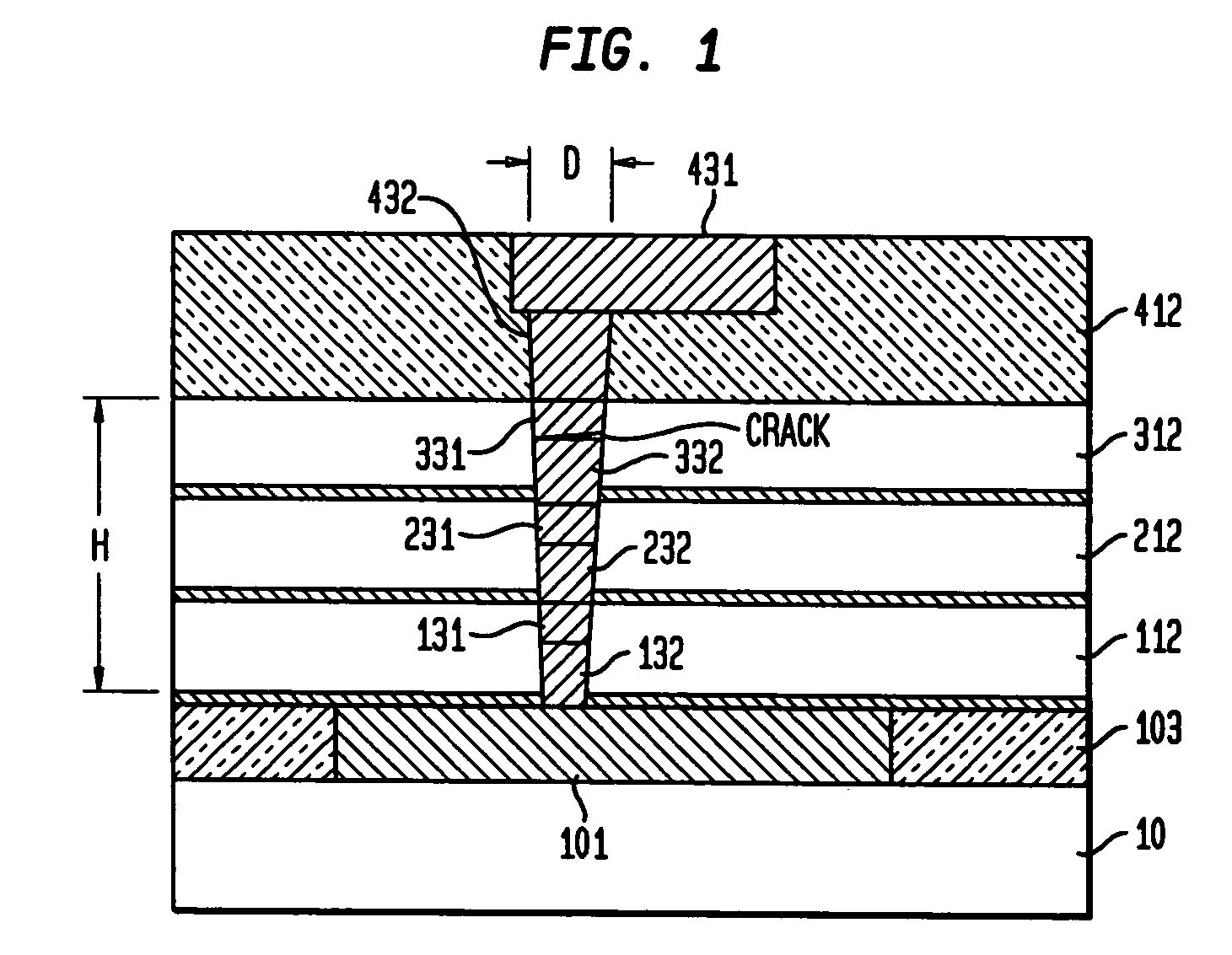
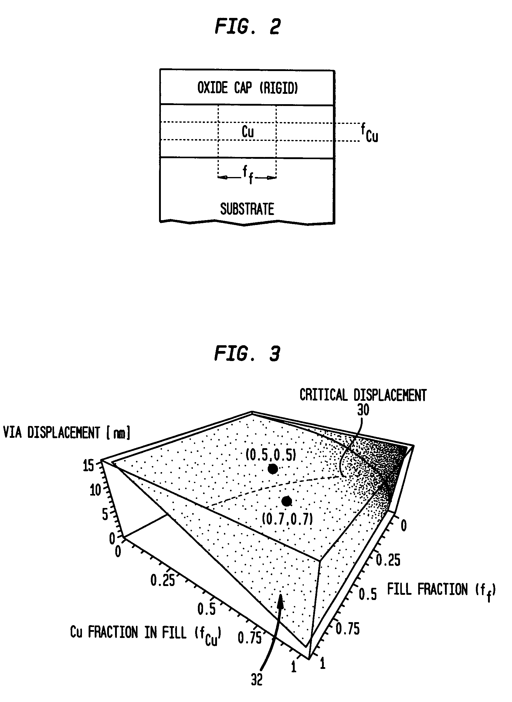
[0037]The present invention provides new semiconductor processes and integrated circuit structures which incorporate stacked via pillars in multilevel interconnection wiring of semiconductor IC (integrated circuit) chips with high conductivity metallurgy such as Cu and low-k inter level dielectrics (ILD), to provide improved structural support and mechanical stability under large thermal excursions.

[0038]The present invention provides for the construction of metal stacked via pillars at different locations in IC chips to support the chip structure during processing and any related processing stresses such as thermal and mechanical stresses. These metal stacked via pillars connect in a straight line from the front end of line (FEOL) up to the far back end of line (FBEOL) and the final step of construction, extending from the base substrate to the top oxide cap.

[0039]The stacked via pillars are not necessarily electrically connected to any active lines or vias, however in some embodim...


PUM


Abstract

Stacked via pillars, such as metal via pillars, are provided at different and designated locations in IC chips to support the chip structure during processing and any related processing stresses such as thermal and mechanical stresses. These stacked via pillars connect and extend from a base substrate of the strip to a top oxide cap of the chip. The primary purpose of the stacked via pillars is to hold the chip structure together to accommodate any radial deformations and also to relieve any stress, thermal and / or mechanical, build-up during processing or reliability testing. The stacked via pillars are generally not electrically connected to any active lines or vias, however in some embodiments the stacked via pillars can provide an additional function of providing an electrical connection in the chip.

Description

BACKGROUND OF THE INVENTION[0001]1. Field of the Invention[0002]The present invention relates generally to new semiconductor processes and integrated circuit structures which provide stacked via pillars in multilevel interconnection structures of semiconductor IC (integrated circuit) chips with high conductivity metallurgy such as copper and low-k dielectrics, to provide improved structural support and mechanical stability under large thermal excursions.[0003]The present invention is particularly applicable to silicon microchip technologies where ruptures in metal interconnects due to thermal expansion can be mitigated by structural support provided by electrically non-functional stacked via pillars and fill patterns.[0004]2. Description of the Prior Art[0005]In order to meet the ever increasing demand for increased device density and performance, a semiconductor technology consisting of a low-k dielectric material and an interconnection wiring of copper metallurgy, defined by a dua...

Claims


Application Information

Patent Timeline
Patent Type & Authority Patents(United States)
IPC IPC(8): H01L29/40H01L21/4763H01L23/00H01L23/58
CPCH01L23/562H01L23/585H01L2924/0002H01L2924/00
Inventor HICHRI, HABIBLIU, XIAO H.MCGAHAY, VINCENT J.MURRAY, CONAL E.NAYAK, JAWAHAR P.SHAW, THOMAS M.
Owner GLOBALFOUNDRIES U S INC
Why Eureka
Try Eureka