Multi-level voltage output control circuit and logic gate therefor

a control circuit and logic gate technology, applied in the direction of logic circuit coupling/interface arrangement, pulse technique, instruments, etc., can solve the problems of increasing power consumption, damage to output performance, and disabling a devi

Active Publication Date: 2006-06-27
MAGNACHIP SEMICONDUCTOR LTD
View PDF4 Cites 9 Cited by
  • Summary
  • Abstract
  • Description
  • Claims
  • Application Information

AI Technical Summary

Benefits of technology

[0014]It is, therefore, an object of the present invention to provide a multi-level voltage output control circuit for removing the occurrence of a penetration current leaking to a low level voltage input terminal when a high level voltage is outputted.
[0015]In accordance with one aspect of the present invention, there is provided a multi-level voltage output control circuit for selectively outputting one of multi-level power voltages by driving gates of two PMOS transistors, which act as switching devices for the multi-level power voltages, with two output signals, wherein the two output signals have complementary phases to each other and generated from two NAND gates coupled with two input signals which have an identical timing and complementary phases to each other. The multi-level voltage output control circuit includes the two NAND gates for advancing a rising timing and slowing down a falling timing of the two output signals, thereby excluding a case in which the two output signals are in a same logic state at the same time, only by modulating sizes of PMOS transistors and NMOS transistors constructing the two NAND gates.
[0018]In accordance with another aspect of the present invention, there is provided a multi-level voltage output control circuit for selectively outputting one of multi-level power voltages by driving gates of two NMOS transistors, which act as switching devices for the multi-level power voltages, with two output signals, wherein the two output signals have complementary phases to each other and generated from two NOR gates coupled with two input signals which have an identical timing and complementary phases to each other. The multi-level voltage output control circuit includes the two NOR gates for slowing down a rising timing and advancing a falling timing of the two output signals, thereby excluding a case in which the two output signals are in a same logic state at the same time, by modulating sizes of PMOS transistors and NMOS transistors constructing the two NOR gates.

Problems solved by technology

The penetration current increases power consumption and makes damage to the output performance and, sometimes, it can disable a device.

Method used


Image

  • Multi-level voltage output control circuit and logic gate therefor
  • Multi-level voltage output control circuit and logic gate therefor
  • Multi-level voltage output control circuit and logic gate therefor

Examples


Embodiment Construction

[0032]Hereinafter, with reference to the drawings, the construction and operation of the present invention will be explained in detail.

[0033]Referring to FIGS. 3A to 3D, the preferred embodiments of the present invention are shown in comparison with the conventional technology. FIGS. 3A and 3C provide representative circuits of the conventional NAND and NOR gates, respectively. FIGS. 3B and 3D show the NAND and NOR gates in accordance with the present invention.

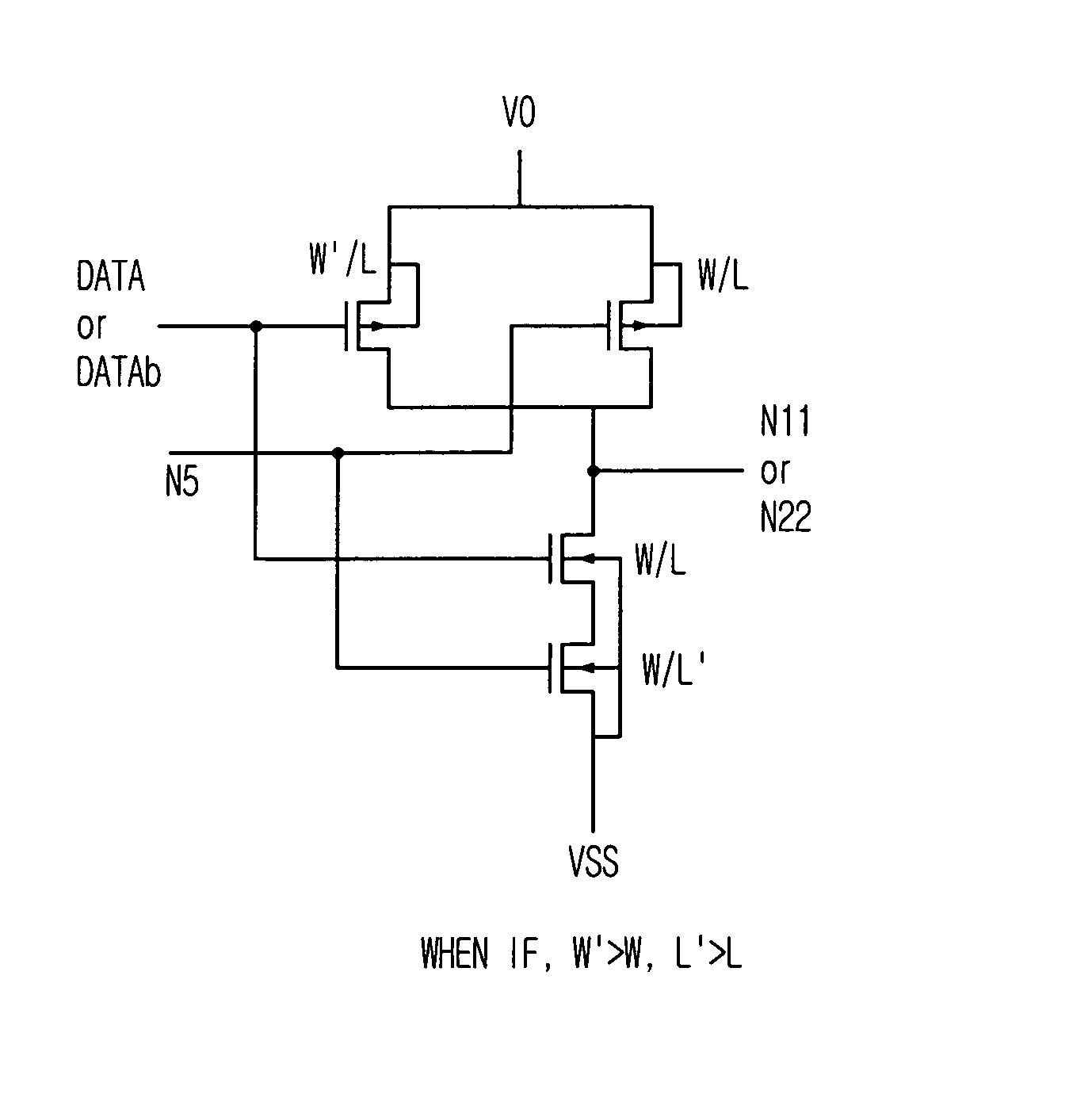
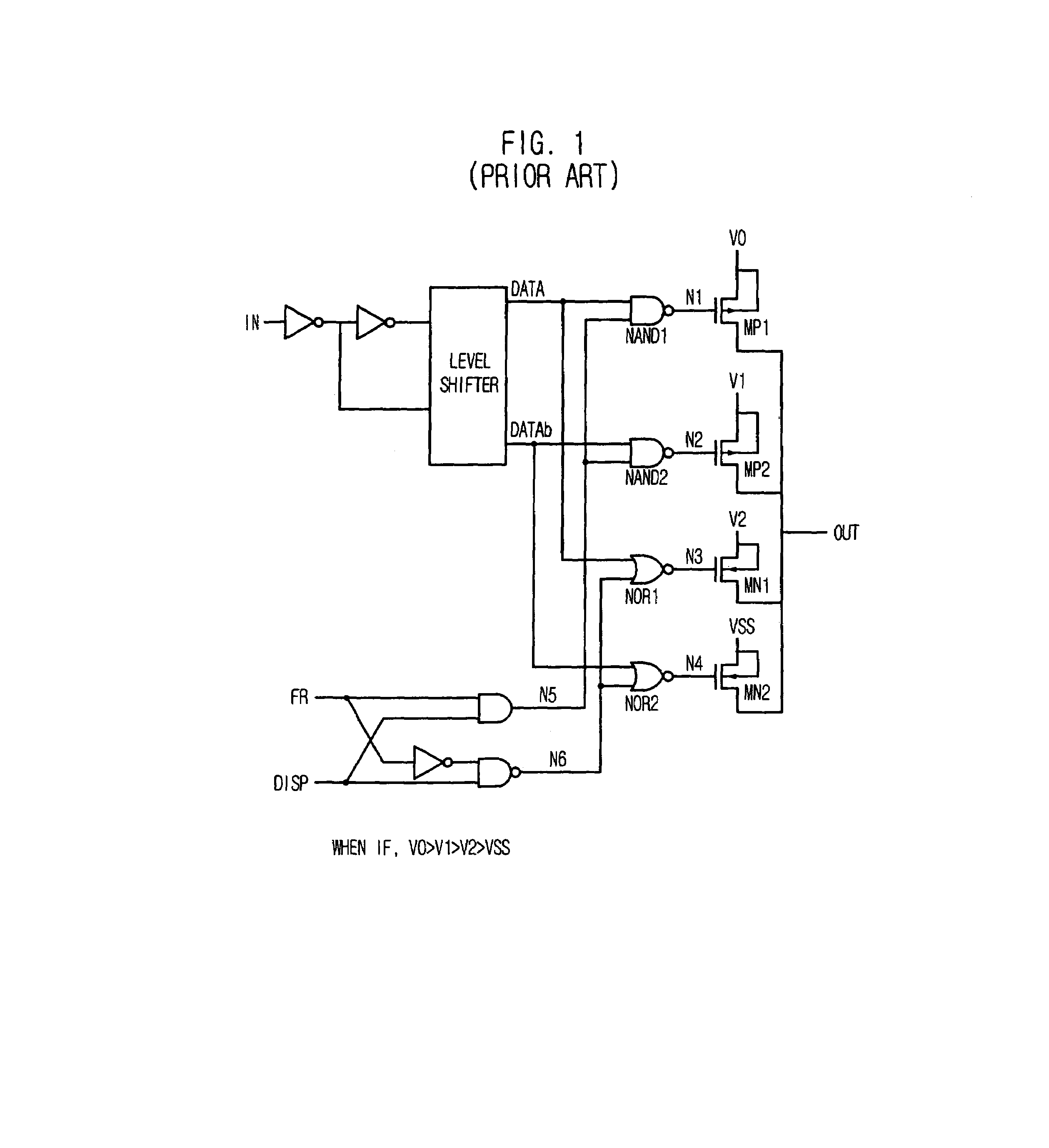
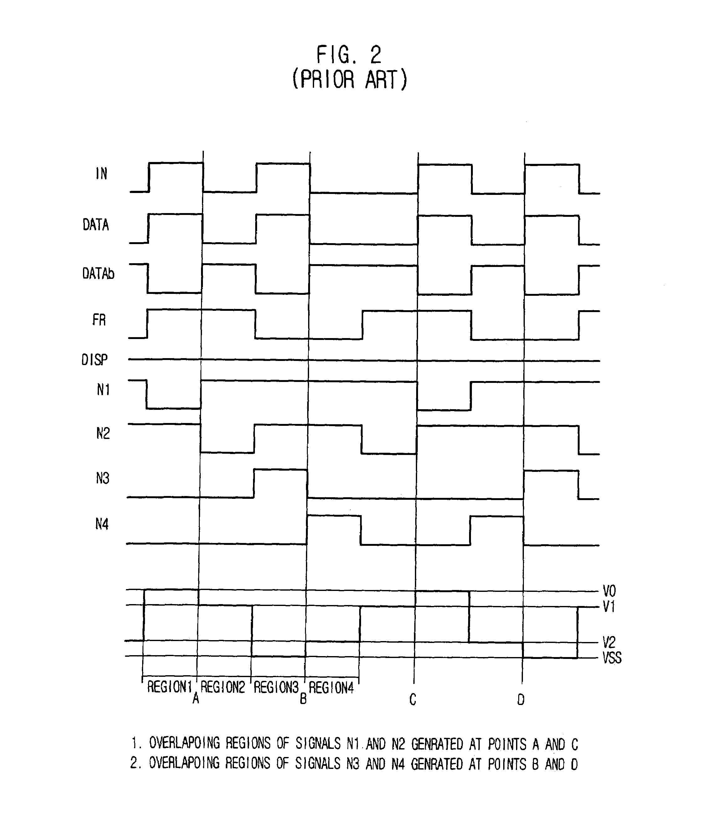
[0034]The logic gates described in FIGS. 3B and 3D are necessarily required in a multi-level voltage output control circuit in accordance with the present invention and are used for driving MOS switching devices which select one of the multi-level voltages in the conventional multi-level voltage output control circuit described in FIG. 1.

[0035]The circuits in FIGS. 3B and 3D are structurally identical to those in FIGS. 3A and 3C, respectively. But, there is a difference in the constitution of MOS transistors constructing the ...


PUM


Abstract

A multi-level voltage output control circuit selectively outputs one of multi-level power voltages by driving gates of two MOS transistors, which act as switching devices for the multi-level power voltages, with two output signals, the two output signals having complementary phases to each other and generated from two logic gates receiving two input signals which have an identical timing and complementary phases to each other, wherein the two logic gates advance or slow down a rising timing and / or a falling timing of the two output signals by differently adjusting a size of PMOS transistors and that of NMOS transistors, which construct the logic gates, thereby excluding a case in which the two output signals are in a same logic state at the same time.

Description

FIELD OF THE INVENTION[0001]The present invention relates to a driving circuit design technology; particularly to a circuit for driving low power in a portable display by removing a penetration current which may be generated at a driving circuit when selecting an output voltage at a multi-level voltage output terminal of a display such as a flat panel display.DESCRIPTION OF RELATED ARTS[0002]In FIG. 1, there is provided a multi-level voltage output control circuit used in a conventional circuit for driving a display such as LCD, PDP and so on.[0003]The multi-level voltage output control circuit includes a multi-level voltage output terminal OUT and switching devices, e.g., transistors MP1, MP2, MN1 and MN2, for selecting a voltage to be outputted through the voltage output terminal OUT. Furthermore, a control unit for controlling the switching of the transistors MP1, MP2, MN1 and MN2 is a logic circuit of NAND gates and NOR gates as shown in FIG. 1.[0004]The NAND gate NAND1 has one ...

Claims


Application Information

Patent Timeline
Patent Type & Authority Patents(United States)
IPC IPC(8): H03K19/094G09G3/36G09G3/20H03K17/00H03K17/16H03K17/687H03K19/00H03K19/0175H03K19/0948
CPCH03K19/0013B43L27/00B24D99/00
Inventor LIM, DAE-HO
Owner MAGNACHIP SEMICONDUCTOR LTD
Why Eureka
Try Eureka