Apparatus and method for use in free-space optical communication comprising optically aligned components integrated on circuit boards
- Summary
- Abstract
- Description
- Claims
- Application Information
AI Technical Summary
Problems solved by technology
Method used
Image
Examples
Embodiment Construction
[0029]The following description is not to be taken in a limiting sense, but is made merely for the purpose of describing the general principles of the invention. The scope of the invention should be determined with reference to the claims.
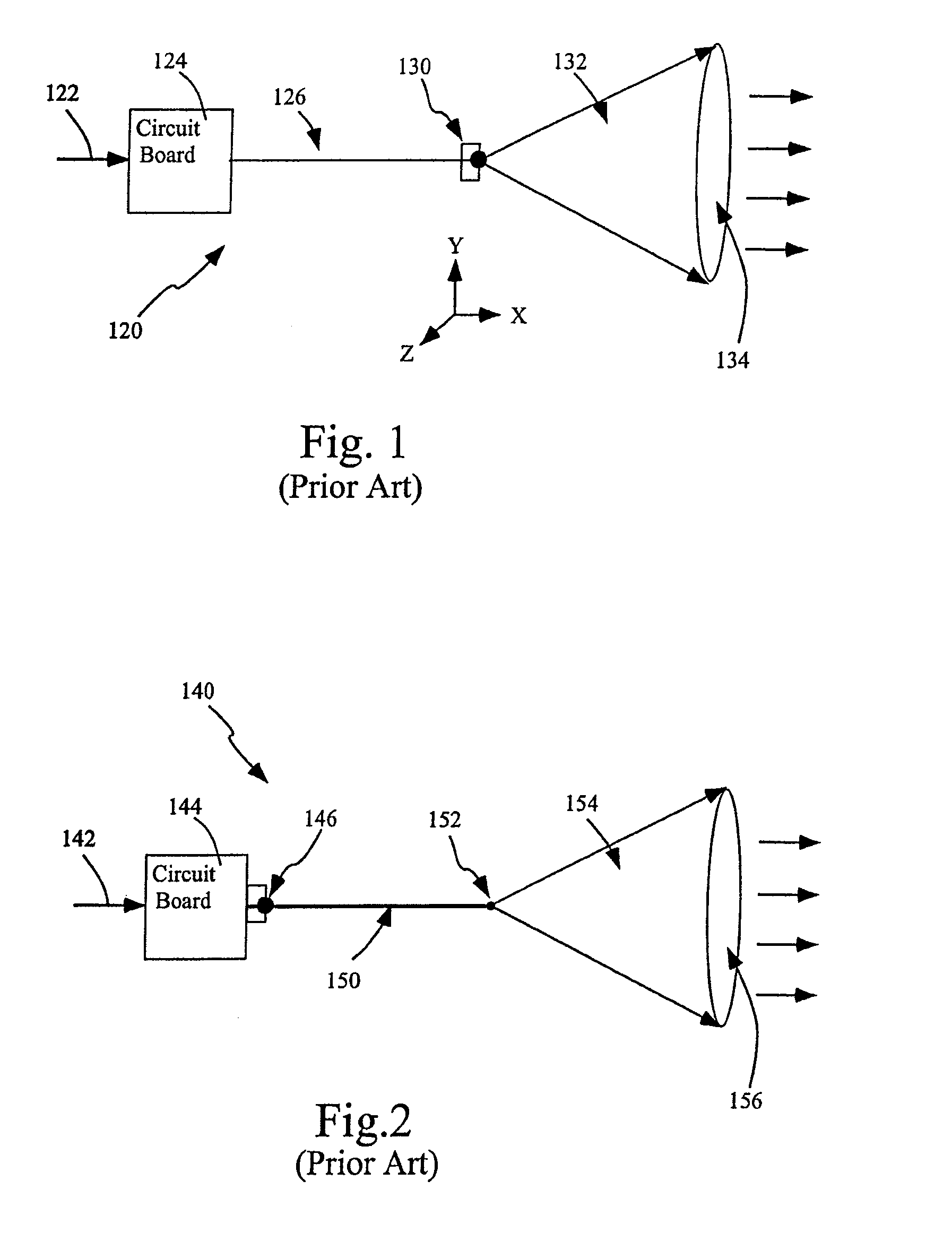
[0030]FIG. 1 depicts a block diagram of a known device 120 for optical communication. The device includes a circuit board 124 receiving signals 122.
[0031]The circuit board generates an electrical drive signal based on the received signal 122 which is used to drive a laser diode 130 or other optical device for generating optical signals. The circuit board couples with a cable or conductor 126, typically a flexible cable. The cable couples with the laser diode 130 to carry the electrical drive signal to the laser diode to drive the diode. The laser diode generates an optical signal 132 that is directed towards a lens 134.
[0032]As is typical with laser diodes, the laser diode 130 is encased in packaging and / or a housing. This requires the step of asse...
PUM
 Abstract
Description
Claims
Application Information


