Semiconductor device package diepad having features formed by electroplating

a technology of electroplating and semiconductor devices, which is applied in the direction of semiconductor devices, semiconductor/solid-state device details, electrical apparatus, etc., can solve the problems of difficult control of the etching stage of the qfn package fabrication process shown in fig. 1f with precision, inability to rapidly and reproducibly stop the progress of chemical etching reaction, and difficulty in forming raised features on the lead frame. to achieve the effect of ensuring the level of the die within the packag

Active Publication Date: 2006-10-17
GEM SERVICES
View PDF8 Cites 37 Cited by
  • Summary
  • Abstract
  • Description
  • Claims
  • Application Information

AI Technical Summary

Benefits of technology

[0019]Embodiments in accordance with the present invention relate to the use of electroplating techniques to form features on the surface of a metal lead frame used in the packaging of semiconductor devices. In accordance with one embodiment, electroplating is used to fabricate portions of the diepad and of the non-integral pins that are shaped to remain securely encapsulated within the plastic molding of the package. In accordance with another embodiment, electroplating may

Problems solved by technology

While adequate for many purposes, the conventional QFN package just described offers some drawbacks.
One drawback is the difficulty of forming raised features on the lead frame.
The etching stage of the QFN package fabrication process shown in FIG. 1F is relatively difficult to control with precision.
This is due to inability to rapidly and reproducibly halt the progress of chemical etching reaction once it is initiated.
Etching outside the above to

Method used


Image

  • Semiconductor device package diepad having features formed by electroplating
  • Semiconductor device package diepad having features formed by electroplating
  • Semiconductor device package diepad having features formed by electroplating

Examples


first embodiment

[0059]In the first embodiment shown in FIGS. 3A–EA, regions of additional thickness of the lead frame corresponding to the exposed lead-posts and diepad are formed by the addition of Cu material. Specifically, a layer of Cu material of precise thickness may be deposited by electroplating over the Cu roll under carefully controlled conditions. The precision of this electroplating process is +1 μm or less. This precision may be compared with conventional etch processes, which exhibit a precision of +25 μm for a Cu substrate having an overall thickness of 4–5 mils. The superior precision of electroplating processes over etching processes may be attributed to the ability to quickly halt electrochemical addition of material reaction by changing the electrical potential.

[0060]The embodiment of the present invention shown in FIGS. 2, and 3A–EA offer a number of advantages. One advantage is relative similarity to the conventional package fabrication process. Specifically, fabrication is acc...

second embodiment

[0071]Owing to this absence of the tie bars, the lead frame of this second embodiment includes four additional pins. These additional pins are located in regions formerly occupied by the tie bars.

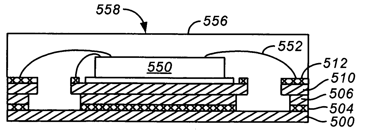
[0072]In step 418 illustrated in FIG. 5I, die 550 is attached to the diepad portion with electrically conducting adhesive, and bond wires 552 are connected between die 550 and the pins. In step 420 illustrated in FIG. 5J, the die / lead frame combination is encapsulated in plastic material 556 while still being supported by the Cu roll 500.

[0073]In step 422 illustrated in FIG. 5K, an array of packages within the encapsulant are separated from the underlying Cu support roll by selective chemical etching. A number of Cu etching techniques are known in the art. One approach involves exposure to aqueous FeCl3, and is described in detail by Duffek and Armstrong, “Etching in Printed Circuit Handbook”—Chapter 6, C. F. Coombs, Ed. (McGraw-Hill, New York, 1967). Another approach involves exposure to a...


PUM


Abstract

Embodiments in accordance with the present invention relate to the fabrication of packages for semiconductor devices, and in particular to the use of electroplating techniques to form features on the surface of a metal lead frame. In accordance with one embodiment, electroplating is used to fabricate non-integral pin portions shaped to remain securely encapsulated within the plastic molding of the package. In accordance with another embodiment, electroplating may be used to fabricate protrusions on the underside of the lead frame for elevating the package above the PC board, thereby preserving the rounded shape of solder balls used to secure the diepad to the PC board. In accordance with yet another embodiment, electroplating may be used to fabricate raised patterns on the upper surface of the diepad for ensuring uniform spreading of adhesive used to secure the die to the diepad, thereby ensuring level attitude of the die within the package.

Description

BACKGROUND OF THE INVENTION[0001]FIG. 1A shows an underside plan view of a conventional quad flat no-lead (QFN) package utilized to house a semiconductor device. FIG. 1B shows a cross-sectional view taken along line B-B′, of the conventional QFN package of FIG. 1A, positioned on a PC board.[0002]QFN package 100 comprises semiconductor die 102 having electrically active structures fabricated thereon. Die 102 is affixed to underlying diepad 104a portion of lead frame 104 by adhesive 106. The relative thickness of the die and lead frame shown in FIG. 1B, and all other drawings of this patent application, is not to scale. Lead frame 104 also comprises non-integral pin portions 104b in electrical communication with die 102 through bond wires 108. Bond wires 108 also allow electrical communication between die 102 and diepad 104a. [0003]Plastic molding 109 encapsulates all but the exposed portions 104a′ and 104b′ of the lead frame portions 104a and 104b, respectively. For the purposes of t...

Claims


Application Information

Patent Timeline
IPC IPC(8): H01L21/44H01L21/48H01L21/50
CPCH01L21/4828H01L21/6835H01L23/49503H01L23/49548H01L23/49582H01L24/48H01L24/83H01L21/568H01L24/32H01L2224/0401H01L2224/05599H01L2224/16H01L2224/32245H01L2224/48091H01L2224/48247H01L2224/48253H01L2224/48257H01L2224/484H01L2224/73253H01L2224/73265H01L2224/8385H01L2224/85001H01L2224/85439H01L2924/01005H01L2924/0102H01L2924/01028H01L2924/01029H01L2924/01046H01L2924/01047H01L2924/01056H01L2924/01075H01L2924/01079H01L2924/01082H01L2924/014H01L2924/07802H01L2924/14H01L2924/15311H01L2924/16195H01L2924/15747H01L2224/16245H01L2924/01033H01L2924/01019H01L2924/01006H01L2924/00014H01L2224/45099H01L2924/00H01L2924/181H01L2924/18301H01L2924/00012
Inventor YILMAZ, HAMZACHIA, ANTHONYFUJIMAKI, SEISHIZENG, XIAOGUANG
Owner GEM SERVICES
Why Eureka
Try Eureka