Structure and method for making strained channel field effect transistor using sacrificial spacer

a technology of strained channel field and transistor, which is applied in the direction of transistors, electrical equipment, semiconductor devices, etc., can solve the problems of limiting the distance between source and drain regions, the threshold voltage of the transistor deviating from a desired value, and the inability to always be desirable for the sige region

Active Publication Date: 2006-11-14
TOSHIBA ELECTRONICS DEVICES & STORAGE CORPORARTION +1
View PDF6 Cites 50 Cited by
  • Summary
  • Abstract
  • Description
  • Claims
  • Application Information

AI Technical Summary

Problems solved by technology

However, it is not always desirable for the SiGe regions of a strained channel transistor structure to coincide with the locations of the source and drain implants.
While the SiGe regions need to be placed close to the channel region to apply the stress needed to obtain high drive current, placed them too close can cause problems such as causing the threshold voltage of the transistor to deviate from a desired value.
However, there is a limit to how close the source and drain regions can be placed to each other.
If they are placed too close to each other, short channel effects occur, which could cause difficulty in turning off the transistor.
When the transistor cannot be fully turned off, excessive leakage current is produced when the transistor is off, causing more power to be consumed even when the transistor is off.
Excessive leakage current can also sometimes cause output signal levels to drift undesirably.

Method used


Image

  • Structure and method for making strained channel field effect transistor using sacrificial spacer
  • Structure and method for making strained channel field effect transistor using sacrificial spacer
  • Structure and method for making strained channel field effect transistor using sacrificial spacer

Examples


Embodiment Construction

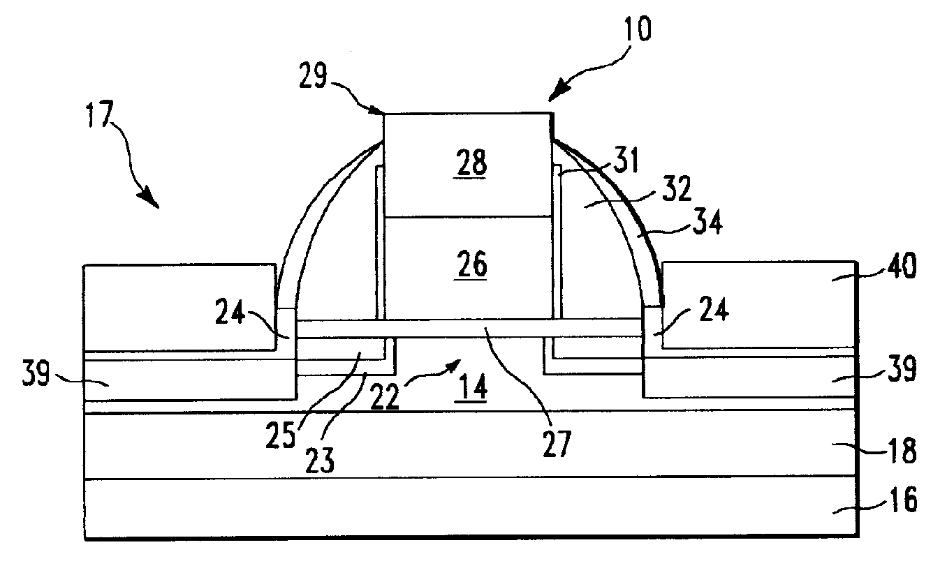
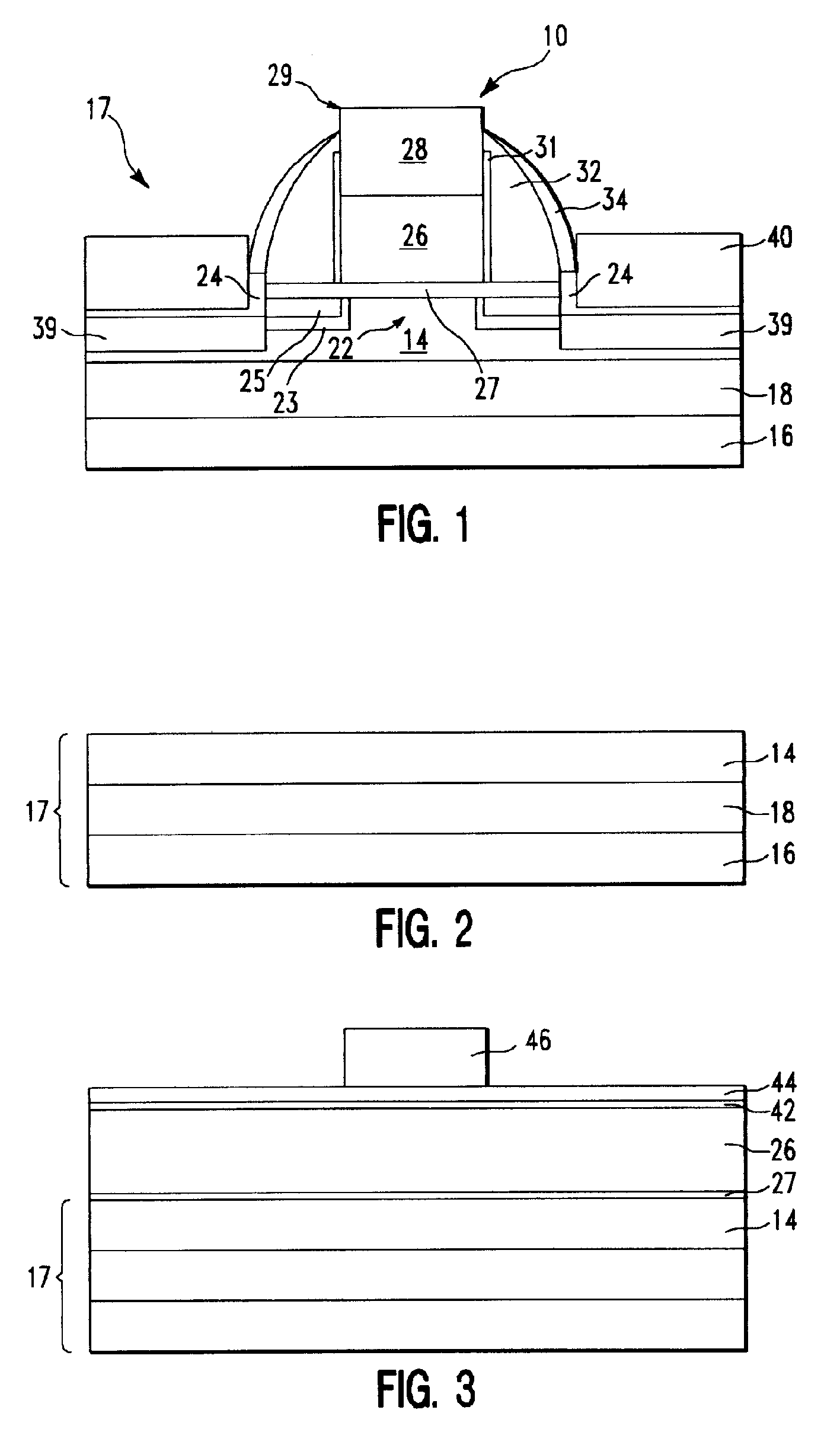
[0012]A strained channel field effect transistor (FET) according to an embodiment of the invention is illustrated in a cross-sectional view, in FIG. 1. The FET 10 is either a PFET having a channel region 22 of p-type conductivity or the FET 10 is an NFET having n-type conductivity. The channel region 22 is disposed below a gate conductor 29 of the FET. When the FET 10 is a PFET, semiconductor alloy regions 39 are placed close to the channel region and apply a compressive longitudinal stress to the channel region 22. Preferably, the channel region 22 is disposed in a region 14 consisting essentially of silicon and the semiconductor alloy regions consist essentially of silicon germanium. Hereinafter, the semiconductor alloy regions 39 are referred to herein as silicon germanium regions 39. The spacing of the silicon germanium regions 39 to the gate conductor 29 is preferably 10 nm or less, in order for the silicon germanium regions 39 to apply a stress having a desirable magnitude to ...


PUM


Abstract

A field effect transistor (“FET”) is provided which includes a gate stack overlying a single-crystal semiconductor region of a substrate, a pair of first spacers disposed over sidewalls of said gate stack, and a pair of regions consisting essentially of a single-crystal semiconductor alloy which are disposed on opposite sides of the gate stack. Each of the semiconductor alloy regions is spaced a first distance from the gate stack. The source region and drain region of the FET are at least partly disposed in respective ones of the semiconductor alloy regions, such that the source region and the drain region are each spaced a second distance from the gate stack by a first spacer of the pair of first spacers, the second distance being different from the first distance.

Description

BACKGROUND OF INVENTION[0001]The present invention relates to the fabrication of semiconductor integrated circuits, and more specifically to an apparatus and method of making a strained channel field effect transistor (FETs) such as an insulated gate field effect transistor (IGFET) in which a stress is applied to the channel region by a semiconductor alloy material disposed adjacent the channel region.[0002]Both theoretical and empirical studies have demonstrated that carrier mobility in a transistor can be greatly increased when a stress of sufficient magnitude is applied to the channel region of a transistor to create a strain therein. Stress is defined as force per unit area. Strain is a dimensionless quantity defined as the change in the dimension of an item, e.g., a change in its length, versus the original dimension, e.g., the original length, when a force is applied in the same direction, i.e., in the direction of its length, in this case. Thus, strain can be either tensile o...

Claims


Application Information

Patent Timeline
Patent Type & Authority Patents(United States)
IPC IPC(8): H01L29/76H01L29/94
CPCH01L21/26506H01L29/6653H01L29/6656H01L29/6659H01L29/66628H01L29/66636H01L29/7848H01L21/28052H01L21/28079H01L21/7624H01L29/1045H01L29/165H01L29/4933H01L29/495H01L29/665H01L29/66545H01L21/18H01L29/772
Inventor CHEN, HUAJIECHIDAMBARRAO, DURESETIOH, SANG-HYUNPANDA, SIDDHARTHARAUSCH, WERNER A.SATO, TSUTOMUUTOMO, HENRY K.
Owner TOSHIBA ELECTRONICS DEVICES & STORAGE CORPORARTION
Why Eureka
Try Eureka