Structure and method for making heterojunction bipolar transistor having self-aligned silicon-germanium raised extrinsic base

a technology of silicongermanium and heterojunction, which is applied in the direction of basic electric elements, electrical apparatus, and semiconductor devices, can solve the problems of high base resistance, large variation in extrinsic base layer thickness, and hence transistor performance, and achieves reduced base resistance, high selectivity, and reduced resistance

Inactive Publication Date: 2006-01-03
INT BUSINESS MASCH CORP
View PDF9 Cites 33 Cited by
  • Summary
  • Abstract
  • Description
  • Claims
  • Application Information

AI Technical Summary

Benefits of technology

[0015]According to preferred aspects of the invention, an HBT is provided which includes a layer of silicon germanium (SiGe) (single-crystal or polycrystalline) as an element of the raised extrinsic base. Such layer is disposed over a relatively thin layer consisting essentially of silicon (single-crystal or polycrystalline silicon) which provides an etch stop layer when the overlying SiGe layer is etched to form an emitter opening. In this manner, a self-aligned transistor is fabricated using a simple method, similar to that of making a non-self-aligned transistor, by plasma etching the SiGe extrinsic base layer selective to the “conductive” silicon stop layer, the plasma etch process having high selectivity. After forming the emitter opening, the thin polysilicon layer is removed in a straightforward manner such that the emitter is formed in the opening thereafter in contact with the intrinsic base. In such manner, the raised extrinsic base is self-aligned to the emitter. Besides simplifying the process of self-aligning the raised extrinsic base, the polycrystalline SiGe layer of the raised extrinsic base reduces the base resistance. Doped polycrystalline SiGe and single-crystal SiGe have lower resistance than comparable doped polysilicon and single-crystal silicon.

Problems solved by technology

A problem of the non-self-aligned structure of HBT 10 is high base resistance.
A drawback of this method is that the extrinsic base layer thickness, hence the transistor performance, can vary significantly between small and large devices, as well as, between low and high density areas of devices due to dishing of the polysilicon during CMP.

Method used


Image

  • Structure and method for making heterojunction bipolar transistor having self-aligned silicon-germanium raised extrinsic base
  • Structure and method for making heterojunction bipolar transistor having self-aligned silicon-germanium raised extrinsic base
  • Structure and method for making heterojunction bipolar transistor having self-aligned silicon-germanium raised extrinsic base

Examples


Embodiment Construction

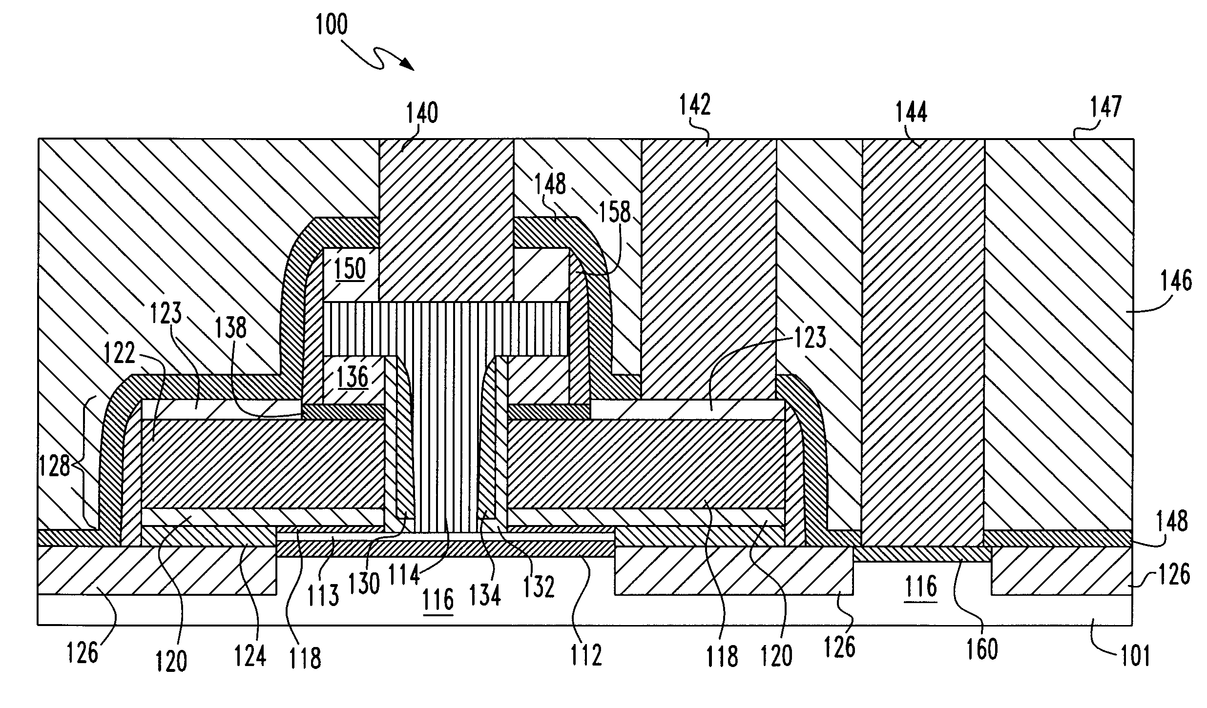
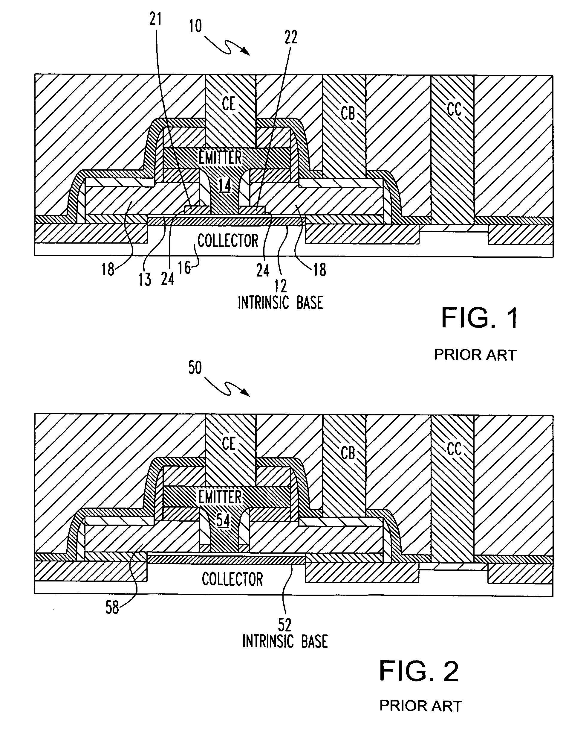
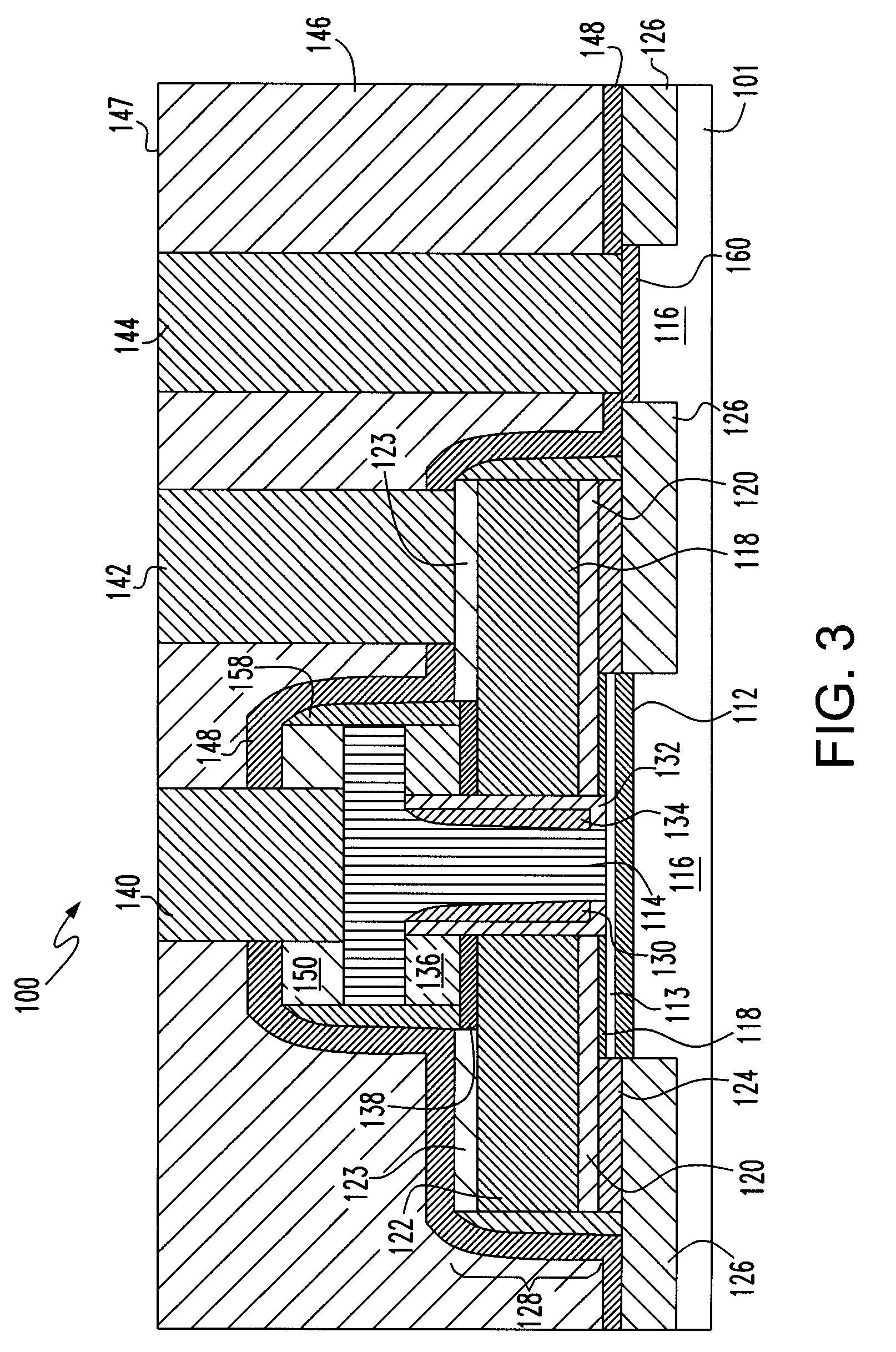
[0023]FIG. 3 is a cross-sectional view illustrating the structure of an HBT 100 according to a first preferred embodiment of the invention. As shown in FIG. 3, HBT 100 is desirably fabricated from a substrate 101, e.g. wafer, of single-crystal silicon. The HBT 100 includes an intrinsic base including a single-crystal layer of silicon germanium 112 disposed over a collector 116 region of the silicon substrate 101. The intrinsic base further includes a single-crystal layer 113 of silicon disposed over the SiGe layer 112. A single-crystal layer 118 of silicon germanium is further disposed over the silicon layer 113. An emitter 114, desirably consisting of polysilicon, contacts the single-crystal silicon layer 113 from above. The raised extrinsic base of the HBT 100 includes SiGe layer 118, polycrystalline silicon layer 120, a polycrystalline SiGe layer 122, and a polycrystalline silicon layer 138 and a silicide layer 123 disposed over portions of the polycrystalline SiGe layer 122. A l...


PUM


Abstract

A heterojunction bipolar transistor (HBT) and method of making an HBT are provided. The HBT includes a collector, and an intrinsic base overlying the collector. The intrinsic base includes a layer of a single-crystal semiconductor alloy. The HBT further includes a raised extrinsic base having a first semiconductive layer overlying the intrinsic base and a second semiconductive layer formed on the first semiconductive layer. An emitter overlies the intrinsic base, and is disposed in an opening of the first and second semiconductive layers, such that the raised extrinsic base is self-aligned to the emitter.

Description

BACKGROUND OF INVENTION[0001]High performance circuits, especially those used for radio frequency chips, favor the use of heterojunction bipolar transistors (HBTs) to provide high maximum oscillation frequency fMAX and cutoff frequency fT. HBTs have a structure in which the base of the transistor includes a relatively thin layer of single-crystal semiconductor alloy material. As an example, an HBT fabricated on a substrate of single-crystal silicon can have a single-crystal base formed of silicon germanium (SiGe) having a substantial proportion of germanium content and profile to improve high speed performance. Such HBT is commonly referred to as a SiGe HBT.[0002]The juxtaposition of alloy semiconductor materials within a single semiconductor crystal is called a “heterojunction.” The heterojunction results in significant quasi-static field that increases the mobility of charge carriers in the base. Increased mobility, in turn, enables higher gain and cutoff frequency to be achieved ...

Claims


Application Information

Patent Timeline
Patent Type & Authority Patents(United States)
IPC IPC(8): H01L29/737H01L21/331H01L29/10H01L29/739
CPCH01L29/1004H01L29/7378H01L29/66242
Inventor CHAN, KEVIN K.KHATER, MARWAN H.SCHONENBERG, KATHRYN T.SIDDHARTHA, PANDA
Owner INT BUSINESS MASCH CORP
Why Eureka
Try Eureka