Multi-junction solar cell device

Inactive Publication Date: 2007-12-18
ALLIANCE FOR SUSTAINABLE ENERGY
View PDF13 Cites 34 Cited by
  • Summary
  • Abstract
  • Description
  • Claims
  • Application Information

AI Technical Summary

Benefits of technology

[0013]The lattice matching condition is temperature dependent because the thermal expansion coefficient of silicon is different from that of III-V semiconductors. Since these III-V semiconductor layers are typically grown at elevated temperatures, it may be more beneficial to lattice match the III-V semiconductor layers to silicon substrates at growth temperature rather than room temperature. When cooled to room temperature, III-V semiconductor layers that have been lattice matched at growth temperature will be slightly lattice mismatched, but should also be considered “substantially lattice matched.”
[0014]In addition, GaP and AlxGa1-xP are only slightly lattice mismatch

Problems solved by technology

Unfortunately, the set of semiconductors alloys (AlGaIn)(PAsSb) cannot be lattice-matched to silicon for any composition.
But because these III-V solar cell designs are not lattice-matched to the un

Method used


Image

  • Multi-junction solar cell device
  • Multi-junction solar cell device

Examples


Embodiment Construction

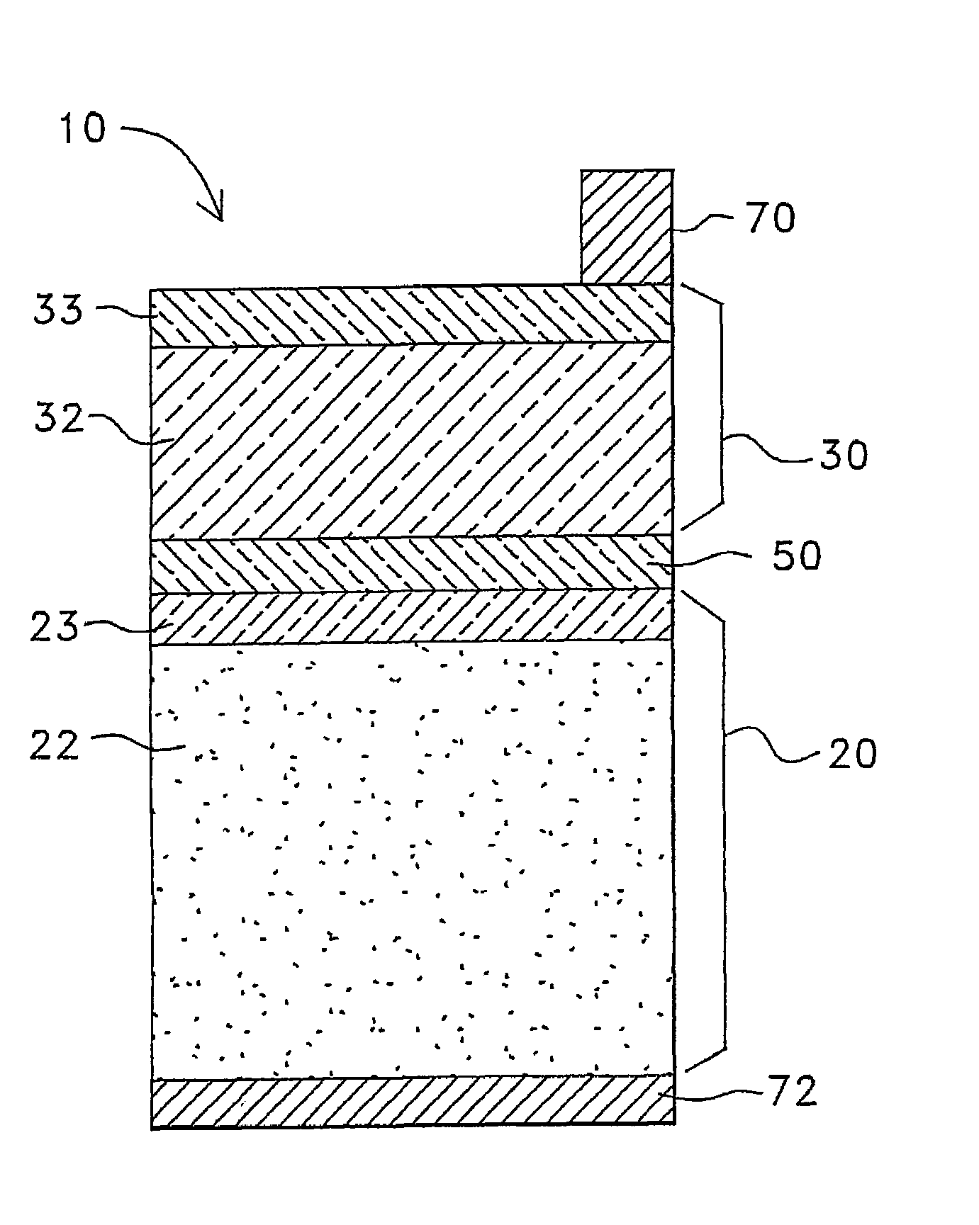
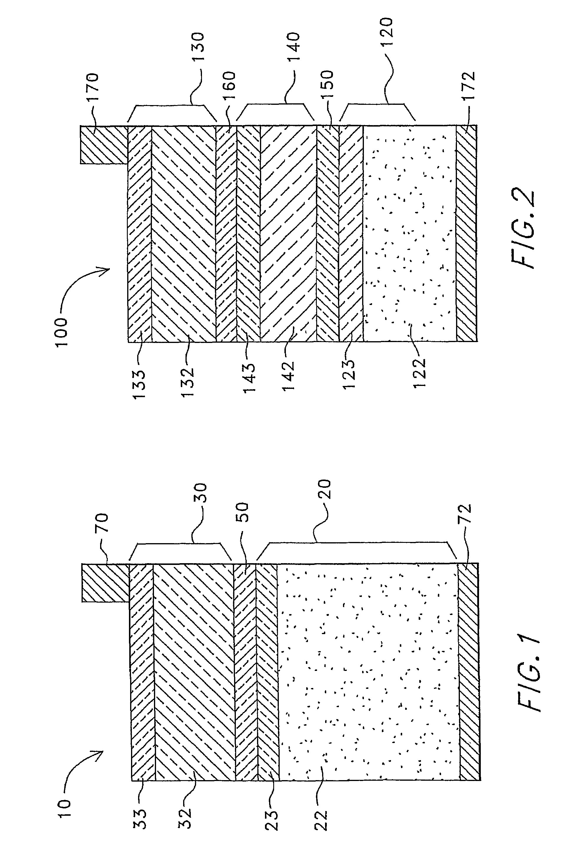
[0018]As illustrated in FIGS. 1 and 2, the present invention is a multi-junction solar cell device, indicated generally in its two-junction version as 10 and in its three-junction version as 100, having lattice-matched (BAlGaIn)(NPAsSb) alloys grown on silicon. The solar cell device 10 rivals the efficiencies of high-efficiency cells on GaAs or Ge, with significant cost savings and improvements in mechanical stability.

[0019]As illustrated in FIG. 1, the two-junction version of the solar cell device 10 of the present invention includes a single-crystal silicon substrate 22. The two-junction device 10 comprises a bottom active cell 20, a top active cell 30, and an interconnecting tunnel junction layer 50. The bottom active cell 20 comprises at least a p-type (or n-type) base layer formed within the silicon substrate 22 and an n-type (or p-type) emitter layer 23 forming a p-n junction. The top active cell 30 comprises at least a p-type (or n-type) base layer 32 and an n-type (or p-type...


PUM


Abstract

A multi-junction solar cell device (10) is provided. The multi-junction solar cell device (10) comprises either two or three active solar cells connected in series in a monolithic structure. The multi-junction device (10) comprises a bottom active cell (20) having a single-crystal silicon substrate base and an emitter layer (23). The multi-junction device (10) further comprises one or two subsequent active cells each having a base layer (32) and an emitter layer (23) with interconnecting tunnel junctions between each active cell. At least one layer that forms each of the top and middle active cells is composed of a single-crystal III-V semiconductor alloy that is substantially lattice-matched to the silicon substrate (22). The polarity of the active p-n junction cells is either p-on-n or n-on-p. The present invention further includes a method for substantially lattice matching single-crystal III-V semiconductor layers with the silicon substrate (22) by including boron and/or nitrogen in the chemical structure of these layers.

Description

CONTRACTUAL ORIGIN OF THE INVENTION[0001]The United States Government has rights in this invention under Contract No. DE-AC36-99GO10337 between the U.S. Department of Energy and the National Renewable Energy Laboratory, a Division of Midwest Research Institute.TECHNICAL FIELD[0002]This invention relates generally to a multi-junction solar cell device and, more particularly, it relates to a multi-junction solar cell device containing III-V layers grown lattice-matched on silicon substrates.BACKGROUND ART[0003]Solar photovoltaic devices, i.e., solar cells, are devices capable of converting solar radiation into usable electrical energy. The energy conversion occurs as the result of what is known as the photovoltaic-effect which occurs in a cell composed of a p-type semiconductor layer adjacent to an n-type semiconductor layer, hereafter referred to as a p-n junction cell. Solar radiation impinging on a solar cell and absorbed by an active region of semiconductor material generates elec...

Claims


Application Information

Patent Timeline
IPC IPC(8): H01L31/00H01L31/0304H01L31/078H01L31/18
CPCH01L31/03046H01L31/0687H01L31/1852H01L31/078Y02E10/544
Inventor FRIEDMAN, DANIEL J.GEISZ, JOHN F.
Owner ALLIANCE FOR SUSTAINABLE ENERGY
Why Eureka
Try Eureka