Method of forming isolation layer of semiconductor device

Inactive Publication Date: 2008-05-01
SK HYNIX INC
View PDF4 Cites 22 Cited by
  • Summary
  • Abstract
  • Description
  • Claims
  • Application Information

AI Technical Summary

Benefits of technology

[0005]One of embodiments of the present invention is directed to a method of forming an isolation layer of a semiconductor device. A void is formed within a trench at

Problems solved by technology

However, as the level of integration of devices increases, the width of each trenc

Method used


Image

  • Method of forming isolation layer of semiconductor device
  • Method of forming isolation layer of semiconductor device
  • Method of forming isolation layer of semiconductor device

Examples


Example

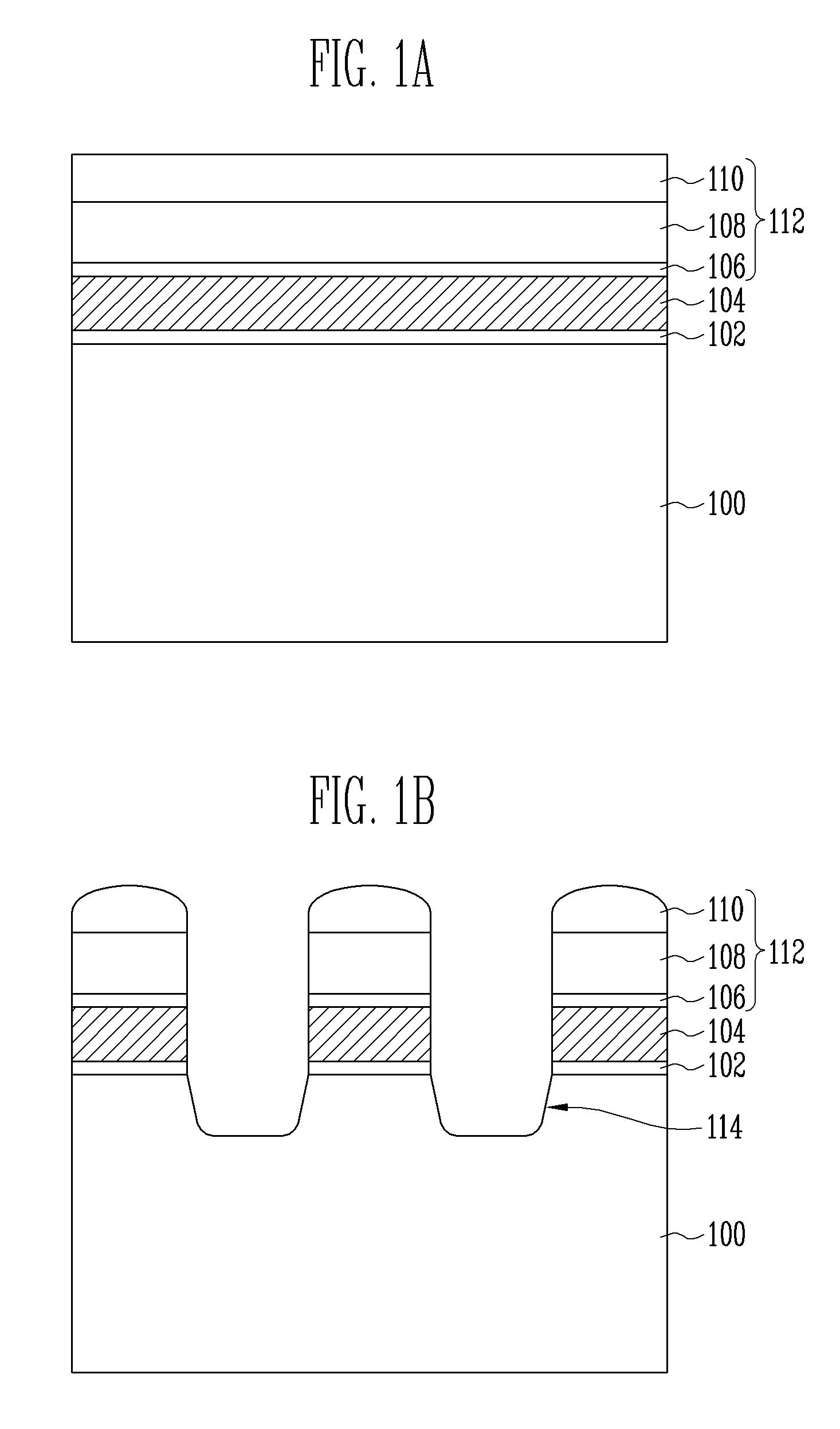
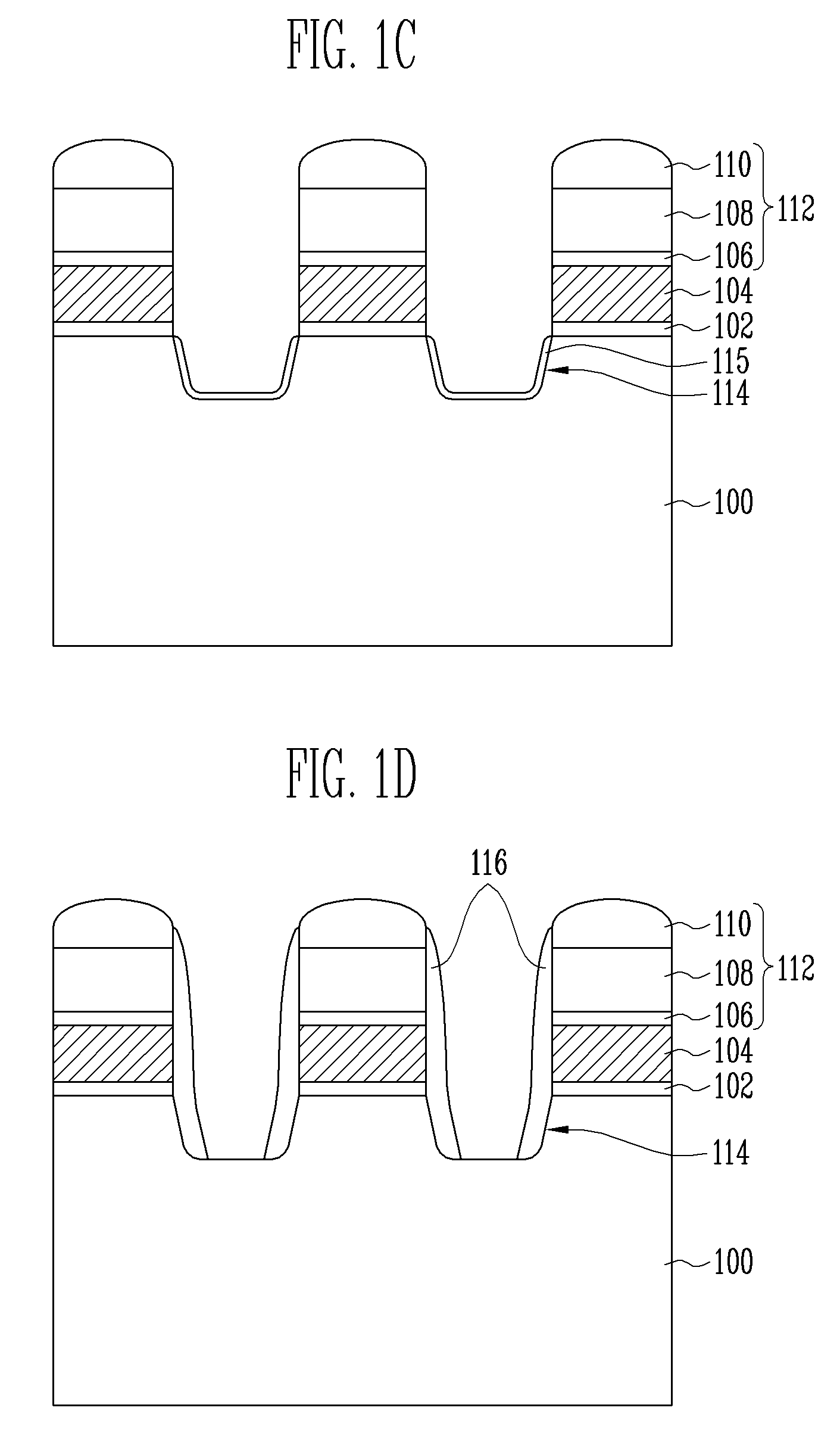
[0013]The present invention will be described in connection with specific embodiments with reference to the accompanying drawings. FIGS. 1A to 1H are cross-sectional views illustrating a method of forming an isolation layer of a semiconductor device according to an embodiment of the present invention.

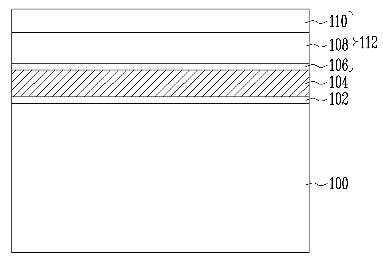
[0014]Referring to FIG. 1A, a tunnel insulating layer 102, an electronic storage layer 104 and an isolation mask 112 are sequentially formed over a semiconductor substrate 100. The isolation mask 112 may comprise a stack of a buffer oxide layer 106, a nitride layer 108 and a hard mask 110. The hard mask 110 may be formed using nitride, oxide, SiON or amorphous carbon. The electronic storage layer 104 forms a floating gate of a flash memory device. The electronic storage layer 104 may be formed using polysilicon or a silicon nitride layer. Alternatively, the electronic storage layer 104 may be formed using any material capable of storing electrons.

[0015]Referring to FIG. 1B, the isolatio...


PUM


Abstract

A method of forming an isolation layer of a semiconductor device includes forming first trenches in an isolation region of a semiconductor substrate. A spacer is formed on sidewalls of each of the first trenches. Second trenches are formed in the isolation region below the corresponding first trenches. Each second trench is narrower and deeper than the corresponding first trench. A first oxide layer is formed on sidewalls and a bottom surface of each of the second trenches. The first trench is filled with an insulating layer.

Description

CROSS-REFERENCES TO RELATED APPLICATIONS[0001]The present application claims priority to Korean patent application number 10-2006-106433, filed on Oct. 31, 2006, which is incorporated herein by reference in its entirety.BACKGROUND OF THE INVENTION[0002]The present invention relates to semiconductor devices and, more particularly, to a method of forming an isolation layer of a semiconductor device employing a Shallow Trench Isolation (STI) process.[0003]In the process of manufacturing semiconductor devices, an isolation layer is formed in order to electrically insulate semiconductor devices (such as transistors) formed over a substrate. Conventionally, the isolation layer was formed by a LOCOS process of a local oxidation method. As the level of integration of devices has increased, the isolation layer is currently formed by a STI process.[0004]The STI process is performed such that an isolation region of a semiconductor substrate is etched to form trenches. The trenches are filled w...

Claims


Application Information

Patent Timeline
IPC IPC(8): H01L21/8242
CPCH01L27/11521H01L21/76232H10B41/30H01L21/76
Inventor DONG, CHA DEOKCHO, WHEE WONKIM, JUNG GEUNJEONG, CHEOL MOKIM, SUK JOONGLEE, JUNG GU
Owner SK HYNIX INC
Why Eureka
Try Eureka