Microphone manufacturing method

Active Publication Date: 2009-07-16
MMI SEMICON CO LTD
View PDF4 Cites 16 Cited by
  • Summary
  • Abstract
  • Description
  • Claims
  • Application Information

AI Technical Summary

Benefits of technology

[0008]In view of the above state of the art, the present invention has been devised, and its object is to provide a microphone manufacturing method that can form a cavit

Problems solved by technology

However, when even a sound pressure is balanced by the bent hole, the vibration film fails to vibrate by the sound pressure.
In this state, the opening area of the cavity on the back face side becomes larger in comparison with the size of the vibration film, thereby making it difficult to manufacture a small-size microphone.
Therefore, in the microphone disclosed in Patent Document 1, even when a bent hole having a great acoustic resistance is achieved, it is difficult to manufacture a small-size microphone.
However, since, upon micr

Method used


Image

  • Microphone manufacturing method
  • Microphone manufacturing method
  • Microphone manufacturing method

Examples


embodiment 1

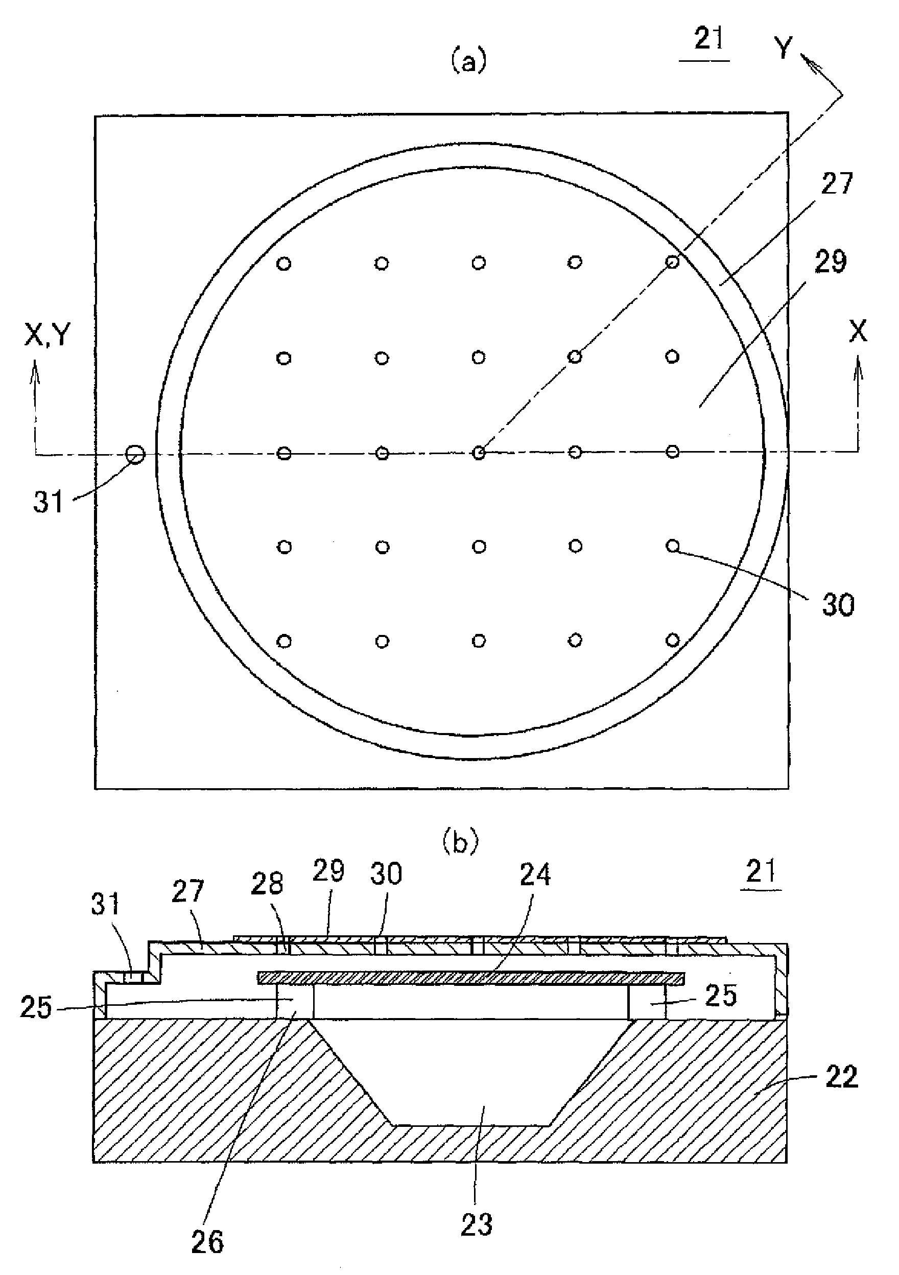
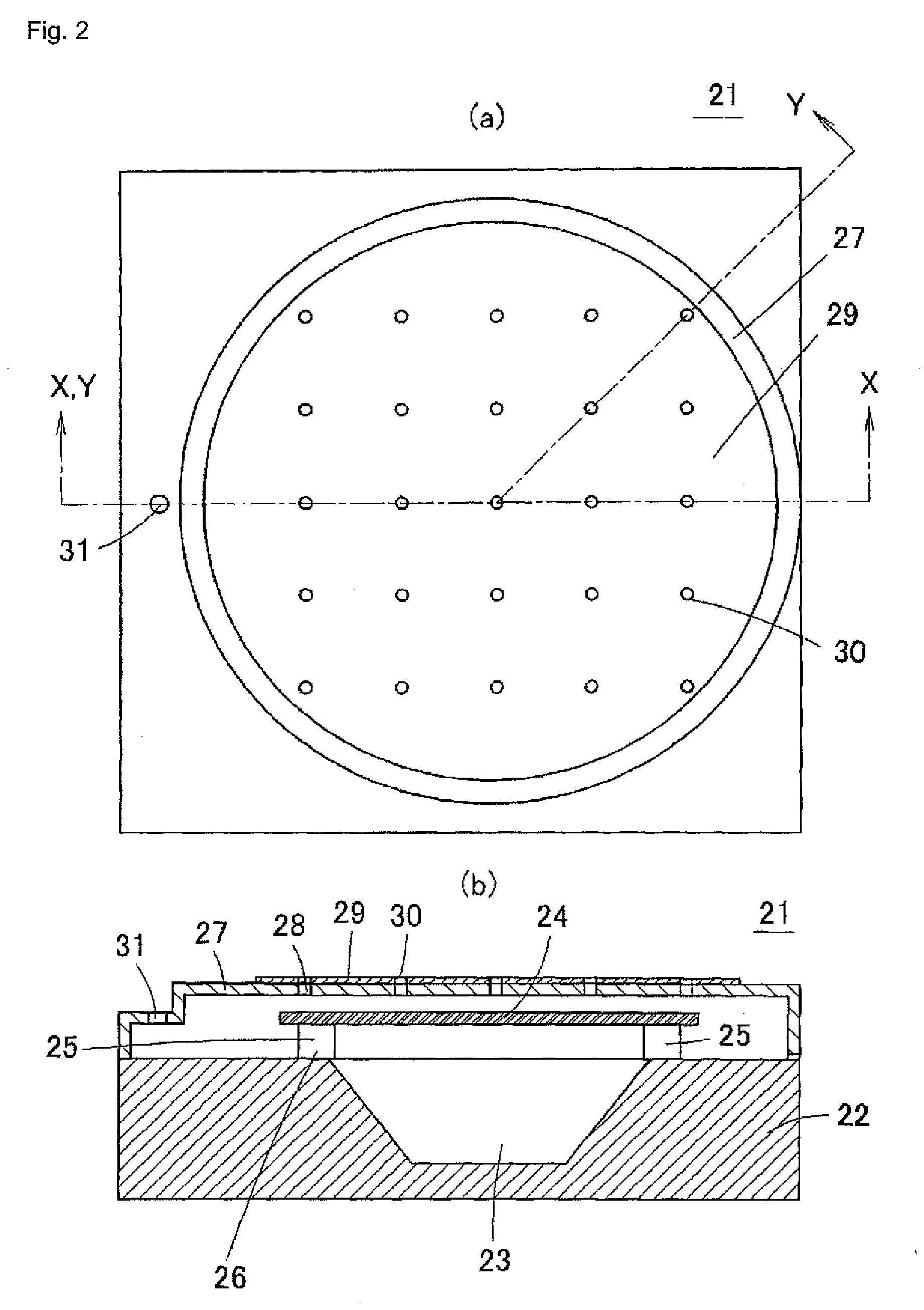
[0062]FIG. 2(a) is a plan view that shows a structure of a microphone 21 in accordance with embodiment 1 of the present invention, and FIG. 2(b) is an X-X line cross-sectional view of FIG. 2(a). Moreover, FIG. 3 is a plan view that shows a microphone 21 from which a back plate has been removed.

[0063]In the microphone 21, a cavity 23 is formed on the surface side of a (100) plane or a (110) plane of the Si substrate 22, and a vibration film 24 is disposed on the Si substrate 22 in such a manner to cover the cavity 23. The cavity 23 is formed by performing crystal anisotropic etching from the surface side of the Si substrate 22, and the peripheral face is formed into a slanting face made of a (111) crystal plane or a crystal plane equivalent thereto, with the opening on the surface side of the cavity 23 being made wider than the bottom face thereof. Four corners of the vibration film 24 are supported by supporting posts 25 formed on the upper surface of the Si substrate 22, with a ben...

embodiment 2

[0097]FIGS. 10(a) to 10(c), FIGS. 11(a) to 11(c) and FIGS. 12(a) to 12(c) are cross-sectional views that show manufacturing processes of a microphone 41 in accordance with embodiment 2 of the present invention. A microphone 41, obtained through these manufacturing processes, makes it possible to eliminate the necessity of a protective film for protecting the vibration film 24 from an etchant upon etching the sacrifice layers 35 and 36 as well as the Si substrate 22; therefore, the film-forming process for the microphone 41 can be simplified. The following description will discuss the manufacturing process thereof.

[0098]First, as shown in FIG. 10(a), a vibration film supporting layer 42 (etching protective film) and a protective film 43, made from SiN, are formed on the surface and the back face of a (100) plane or a (110) plane of an Si substrate 22 (wafer). Next, on the surface of the Si substrate 22, the vibration film supporting layer 42 on an area where a cavity 23 is to be form...

embodiment 3

[0110]FIG. 13(a) is a plan view that shows a structure of a microphone 51 in accordance with embodiment 3 of the present invention, and FIG. 13(b) is a Z-Z line cross-sectional view of FIG. 13(a). This microphone 51 is characterized by adding a functional unit, such as a wrinkle (crease) structure and a stopper 52, to the vibration film 24.

[0111]The wrinkle structure of the vibration film 24 is formed by a bent portion 53 having a square ring shape. The bent portion 53 is bent so as to protrude toward the upper face side of the vibration film 24 in its cross section. By forming this wrinkle structure in the vibration film 24 in this manner, the positional change of the vibration film 24 is increased and the deflection due to a stress is reduced, and these facts are reported by “The fabrication and use of micromachined corrugated silicon diaphragms” (J. H. Jerman, Sensors and Actuators A21-A23 pp. 998-992, 1992).

[0112]The stopper 52 is formed by allowing the surface of the vibration ...


PUM

PropertyMeasurementUnit
Electrical resistanceaaaaaaaaaa

Abstract

A sacrifice layer 36 is exposed through a chemical charging port 31 so that the sacrifice layer 36 and sacrifice layer 35 are etched and removed by an etchant introduced from the chemical charging port 31. Since the surface of an Si substrate 22 is exposed to an etching window 34 corresponding to the removed portion of the sacrifice layer 35, the Si substrate 22 is crystal anisotropically etched below the etching window 34 to form a cavity 23. In contrast, in a space corresponding to the etched and removed portion of the sacrifice layer 36, since the surface of the Si substrate 22 is covered with a protective film 32, the Si substrate 22 is not etched to form a bent hole 26 therein. The cavity can be formed in the semiconductor substrate by an etching process from the surface side. Moreover, a bent hole having a great acoustic resistance can be easily formed.

Description

TECHNICAL FIELD[0001]This invention relates to a microphone manufacturing method, and specifically a small-size microphone manufacturing method, in which a vibration film is formed on a semiconductor substrate.BACKGROUND ART[0002]In a microphone, when a static pressure difference occurs between upper and lower spaces of a vibration film, the vibration film is warped due to the static pressure difference, and the sensitivity of the microphone is thus lowered. For this reason, a bent hole that aims to balance the static pressures is sometimes formed between the semiconductor substrate and the vibration film.[0003]However, when even a sound pressure is balanced by the bent hole, the vibration film fails to vibrate by the sound pressure. Therefore, the bent hole is desirably formed as a passage having a high acoustic resistance. The acoustic resistance becomes higher as the cross-sectional area of the passage becomes smaller and the length thereof becomes longer. For this reason, in ord...

Claims


Application Information

Patent Timeline
IPC IPC(8): H01L21/302
CPCH04R31/00H04R19/005Y10T29/49005Y10T29/49002Y10T29/4908H04R19/04
Inventor HORIMOTO, YASUHIROKASAI, TAKASHI
Owner MMI SEMICON CO LTD
Why Eureka
Try Eureka