

Piezoelectric thin film resonators
- Summary
- Abstract
- Description
- Claims
- Application Information
AI Technical Summary
Benefits of technology
Problems solved by technology
Method used
Image

Examples
example 1
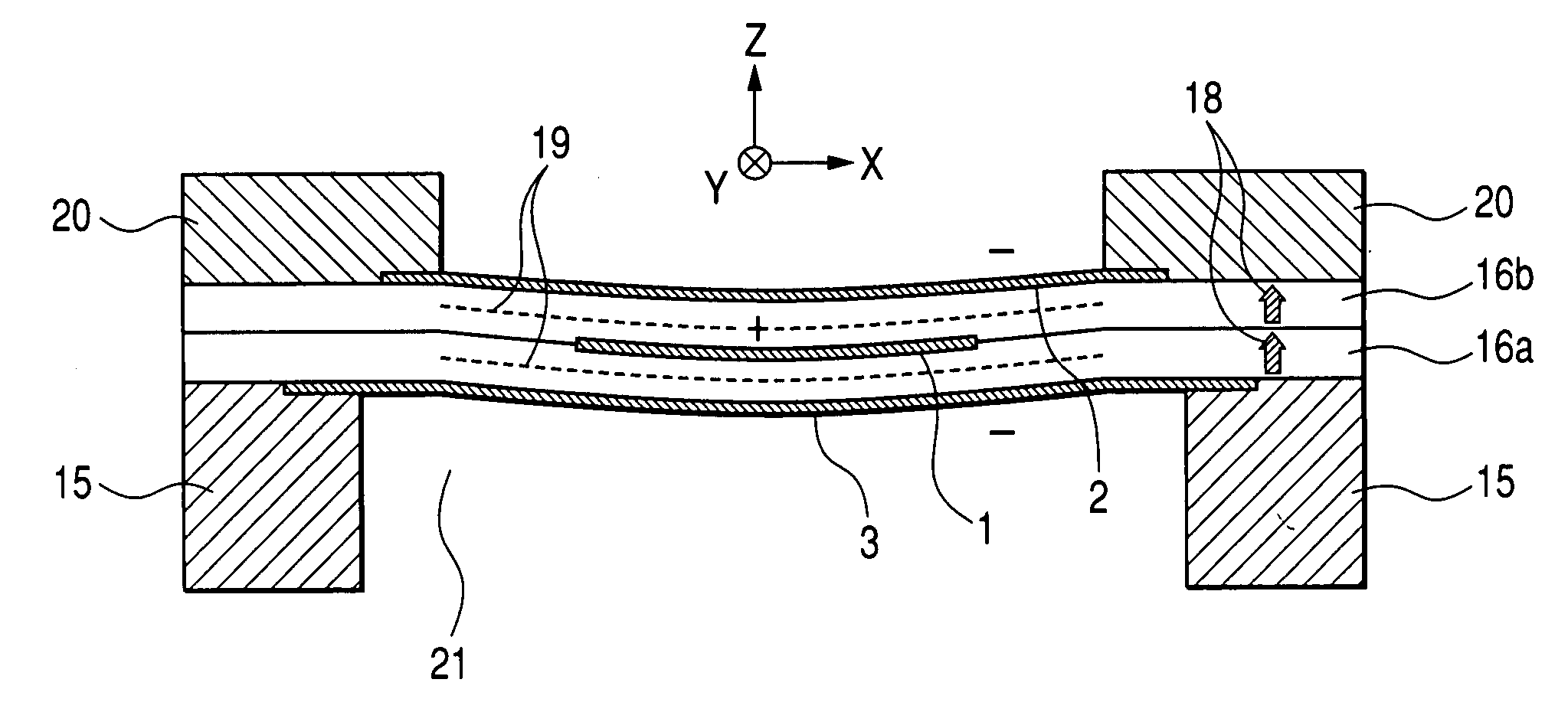
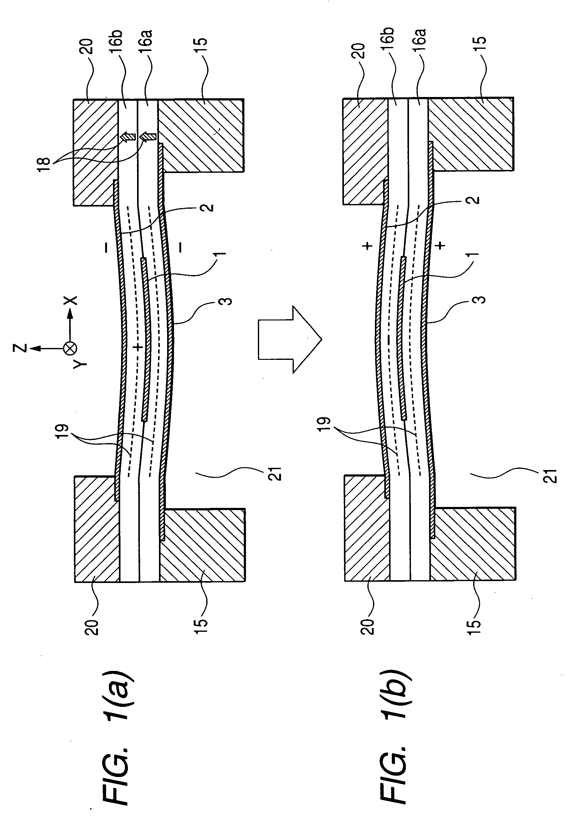
[0059]FIGS. 1A, 1B are cross sectional structural views showing a first embodiment of a resonator according to the invention. At first, the basic constitution and the principle of the invention are to be described based on the drawing. In FIGS. 1A, 1B, two layers of piezoelectric dielectric thin films having identical direction of polarization 18, that is, piezoelectric thin films 16a, 16b are formed above a base substrate 15 such as made of Si. An electrode 1 is disposed between two sheets of piezoelectric thin films 16a and 16b, and electrodes 2, 3 are formed on the upper and lower piezoelectric thin films while sandwiching them. Reference 18 in the drawing shows polarization of the piezoelectric thin film 16 and 20 shows a clamp pattern respectively.
[0060] When a high frequency voltage is applied between the electrode 1 and the electrodes 2, 3, in the case of FIG. 1A where the electrode 1 is at a positive and electrodes 2, 3 are at a negative potentials, since the direction of t...
example 2
[0074]FIGS. 5A, 5B, FIGS. 6A, 6B, and FIGS. 7A, 7B show other examples of the invention. Generally, piezoelectric materials such as AlN, metal materials constituting the electrode, etc. have negative temperature characteristics that the acoustic velocity lowers as the temperature is higher. This means that a resonance frequency lowers as a temperature goes higher in a case of forming a resonator. Because of the negative temperature coefficient, the application use is restricted in a case of constituting a resonator by using the resonator of the invention shown in Example 1. Examples of FIGS. 5A, 5B, FIGS. 6A, 6B and FIGS. 7A, 7B solve such problem.
[0075] There is a material in which the acoustic velocity increases as the temperature goes higher such as silicon oxide (SiO2), also this is an exceptional example. FIGS. 5A, 5B show an example of forming a dielectric film 7 for temperature compensation such as a SiO2 film having a temperature characteristic opposite to that of AlN to th...
example 3
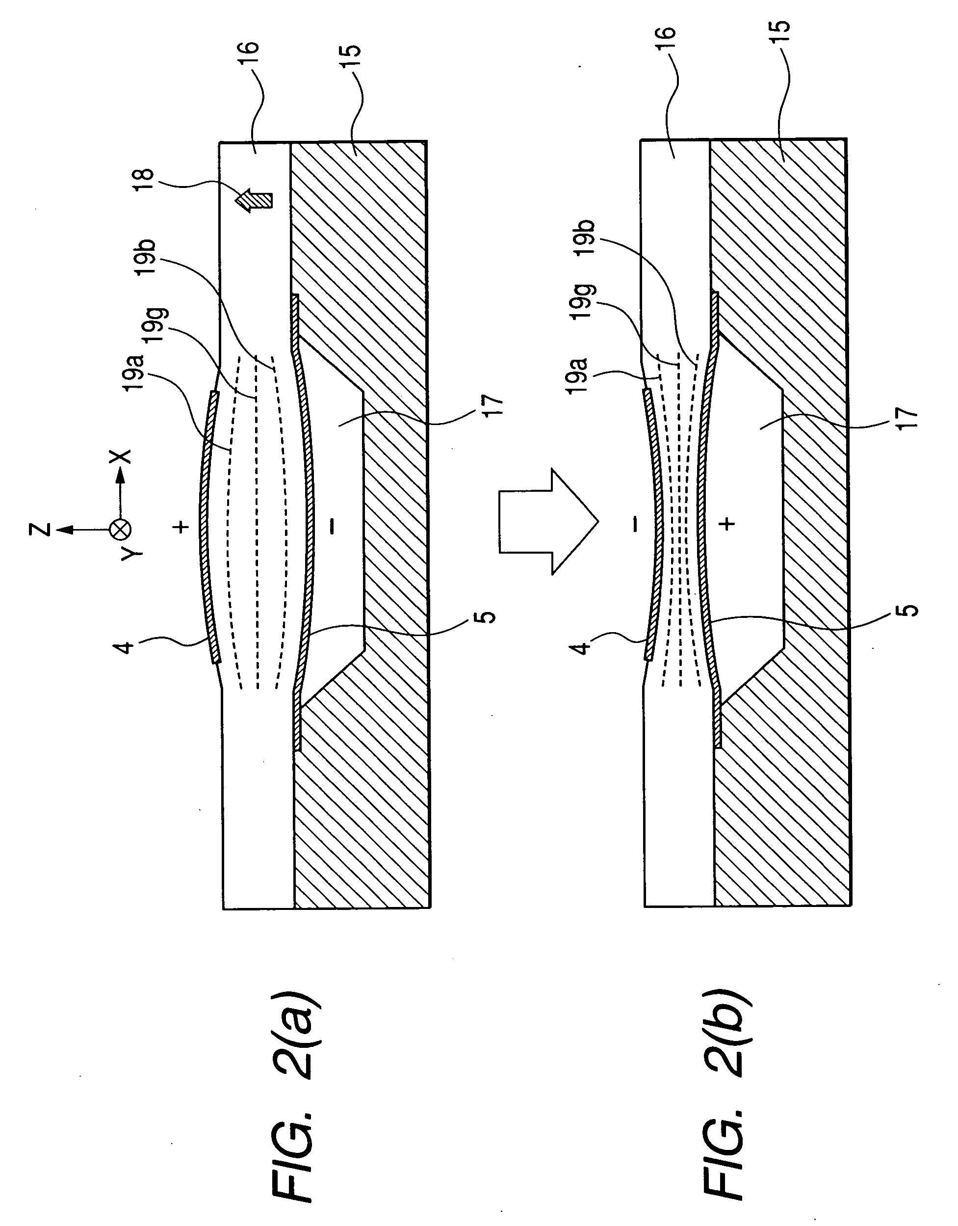
[0078]FIGS. 8A, 8B, FIGS. 9A, 9B, and FIGS. 10A, 10B show other examples of the invention. In FIG. 8A, 8B, one of the two layers of dielectric thin films is removed (end of the piezoelectric thin film 16b of the upper layer is removed in this example) and a gap 22 is provided to decrease the thickness of the piezoelectric thin film in an equivalent manner. This intends to prevent the energy of oscillations from leaking by way of the clamp pattern 20 and to improve the Q value of the resonator.
[0079] Further, in FIGS. 9A, 9B, a temperature compensation film is further introduced to the constitution of FIGS. 8A, 8B intending to improve both the temperature characteristic in FIGS. 5A, 5B and improve the Q value in FIGS. 8A, 8B together.
[0080] Further more, in FIGS. 10A, 10B, the number of layers of the thin films is decreased near the clamp pattern 20 in the same manner as described above, but the thin film is fixed by the clamp pattern 20 by way of the dielectric film 7 for temperat...
PUM
 Abstract
Description
Claims
Application Information