

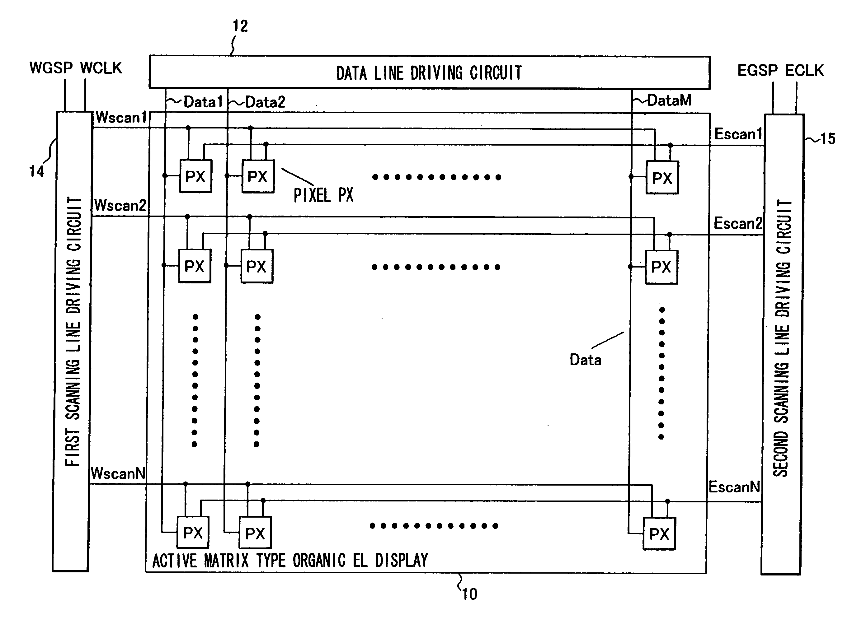
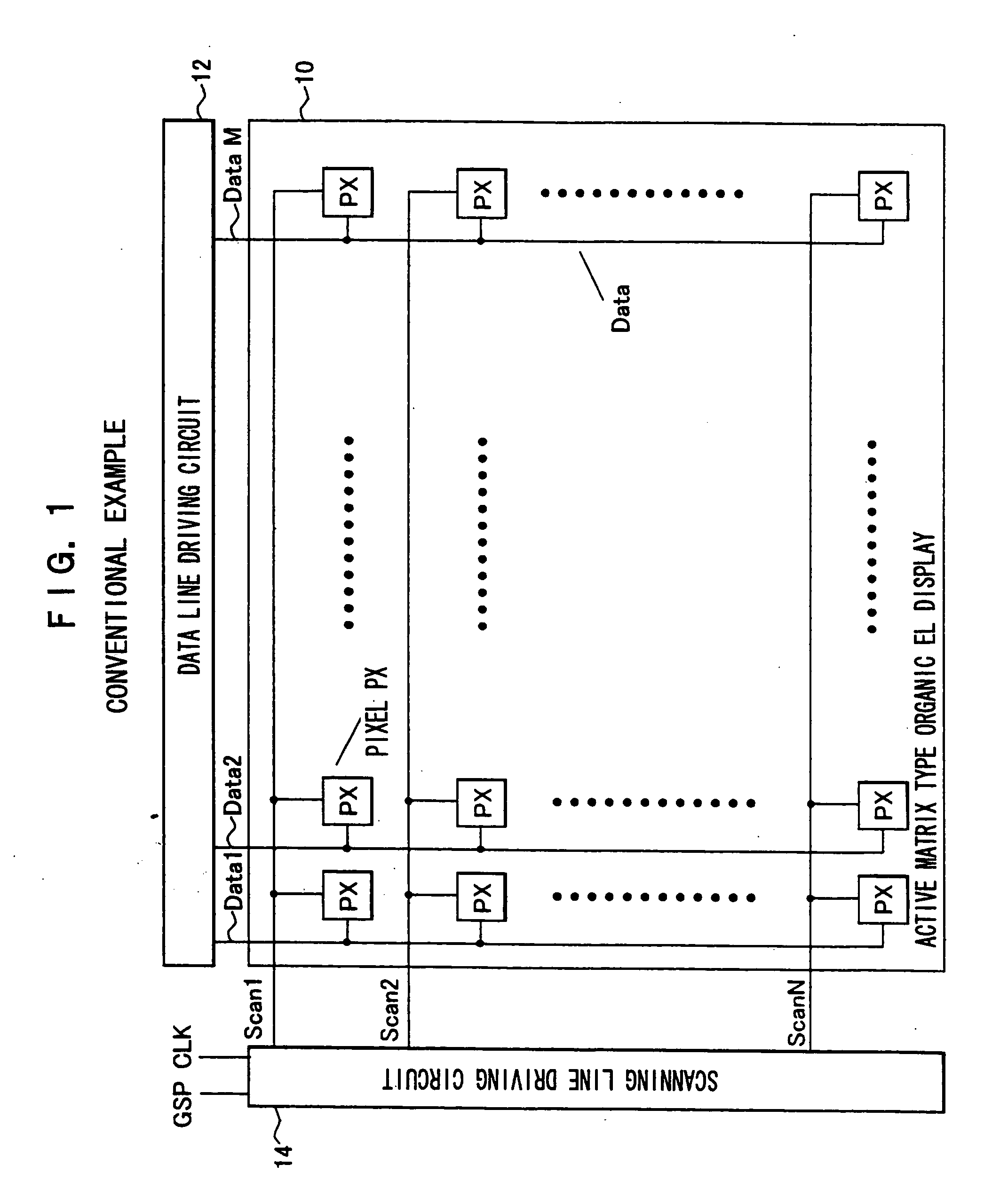
Active Matrix Type Display Device
- Summary
- Abstract
- Description
- Claims
- Application Information
AI Technical Summary
Benefits of technology
Problems solved by technology
Method used
Image

Examples
modified example
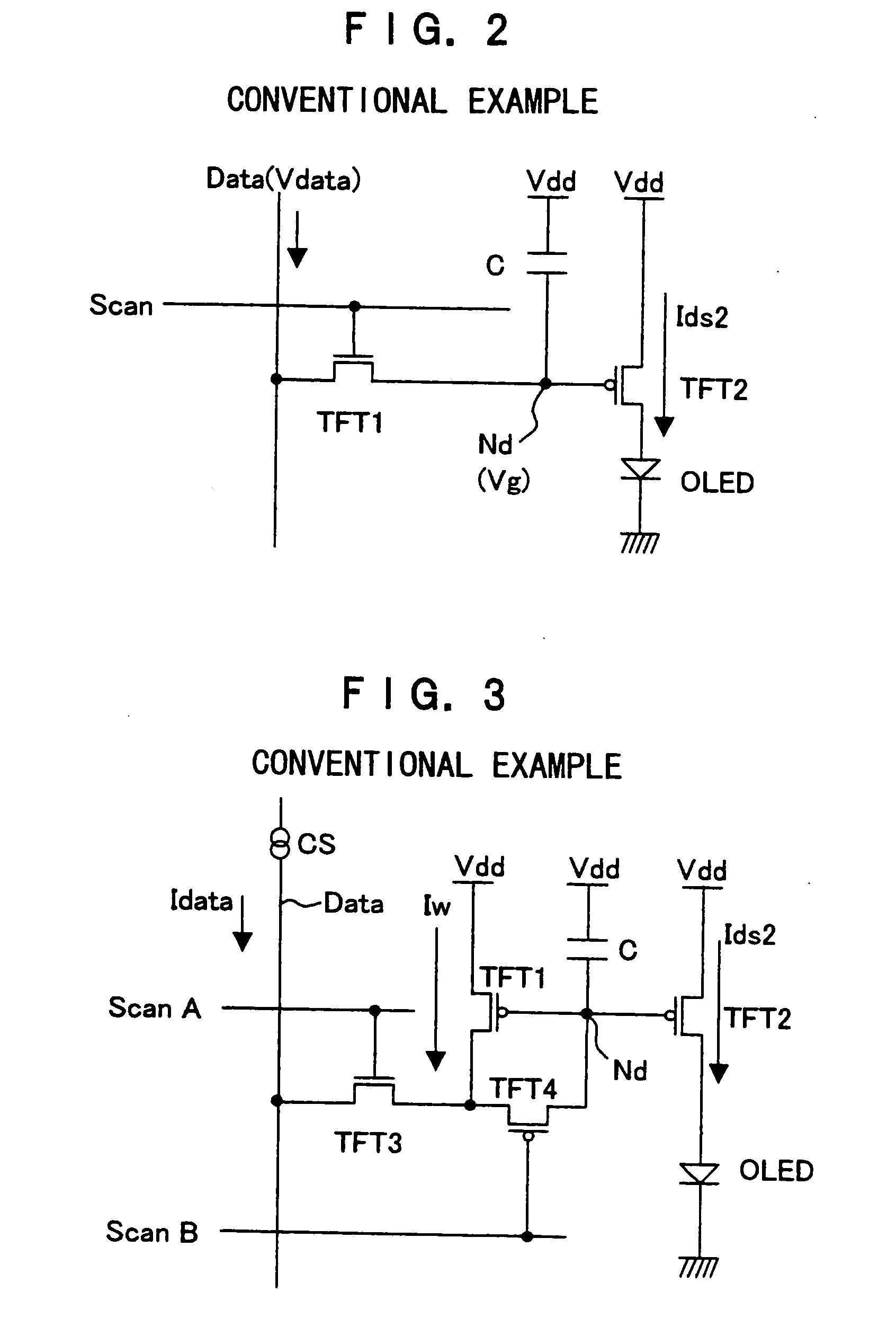
[0061]FIG. 12 shows a modified example of an embodiment of the invention. The pixel circuit of the modified example uses a MOS transistor having a double gate structure as the second transistor TFT2. The second transistor TFT2 is controlled to be in an off-state in response to the L level of the second scanning line Escan during the reading period and the capacitor C maintains a charged state. Accordingly, occurrence of current leakage from the node Nd, which tends to cause fluctuations of the display brightness, has to be avoided as much as possible. Therefore, in this modified example, two gate electrodes are formed in the second transistor TFT2 and both of these two gate electrodes are connected to the second scanning line Escan. As a result, both of the two gate electrodes are controlled to the L level and the current leakage in the off-state can be suppressed.
PUM
 Abstract
Description
Claims
Application Information