Method of and apparatus for automatically correcting device model, and computer product

Inactive Publication Date: 2006-11-14
FUJITSU LTD
View PDF14 Cites 8 Cited by
  • Summary
  • Abstract
  • Description
  • Claims
  • Application Information

AI Technical Summary

Benefits of technology

[0021]It is an object of this invention to provide an automatic device model correcting program, an automatic device model correcting apparatus, and an automatic device model correcting method capable of quickly and accurately checking a device model and correcting a defective section without depending on the user skill.

Problems solved by technology

Therefore, a problem occurs that a trouble occurs in a printed circuit board concerned serving as an actual model even if there is no problem in circuit design and transmission simulation.
Therefore, when supplying the spice model to an electronic maker, the process parameter and configuration of a circuit included in the company secret of a semiconductor vendor is opened to the public and thereby, a state undesirable for the semiconductor vendor occurs.
As described above, an IBIS model including trouble information may be conventionally supplied to an electronic maker due to erroneous setting of or insufficient checking by a conversion tool when converting a spice model to an IBIS model.
In this case, because an electronic maker executes circuit design and transmission simulation by using an IBIS model including trouble information, a critical problem occurs that a trouble occurs in a printed circuit board serving as an actual model.
Therefore, in the case of an electronic maker insufficient in the number of talents having the user skill, it is substantially difficult to perform checking and correction of trouble information and the maker cannot find a trouble until a trouble occurs in a printed circuit board serving as an actual model and then it cannot be helped to take a post-action that the maker requests a semiconductor vendor to specify and correct a defective section of an IBIS model.
Therefore, it is conventionally difficult to completely correspond to the needs of designing a printed circuit board in a short period.

Method used


Image

  • Method of and apparatus for automatically correcting device model, and computer product
  • Method of and apparatus for automatically correcting device model, and computer product
  • Method of and apparatus for automatically correcting device model, and computer product

Examples


Embodiment Construction

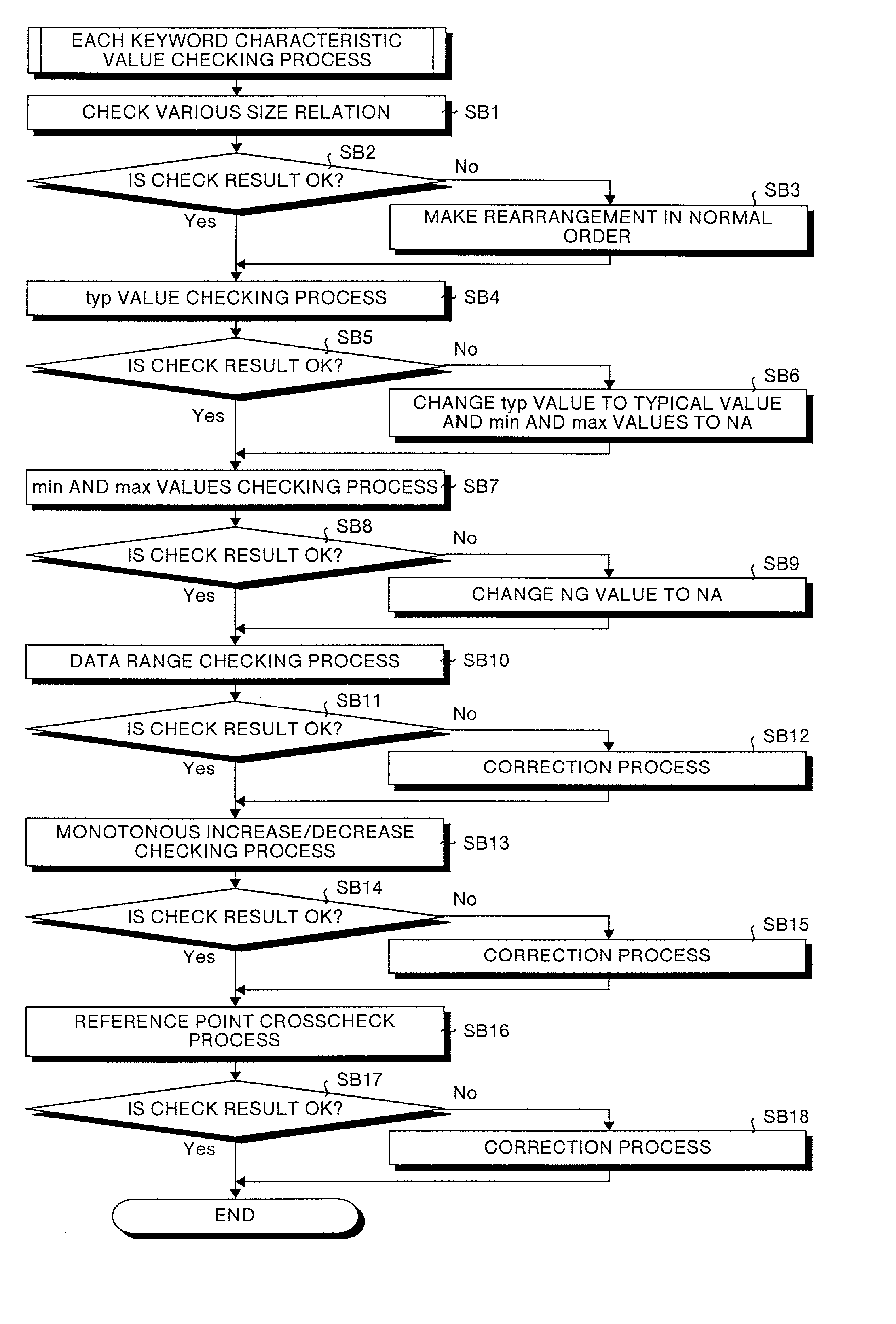
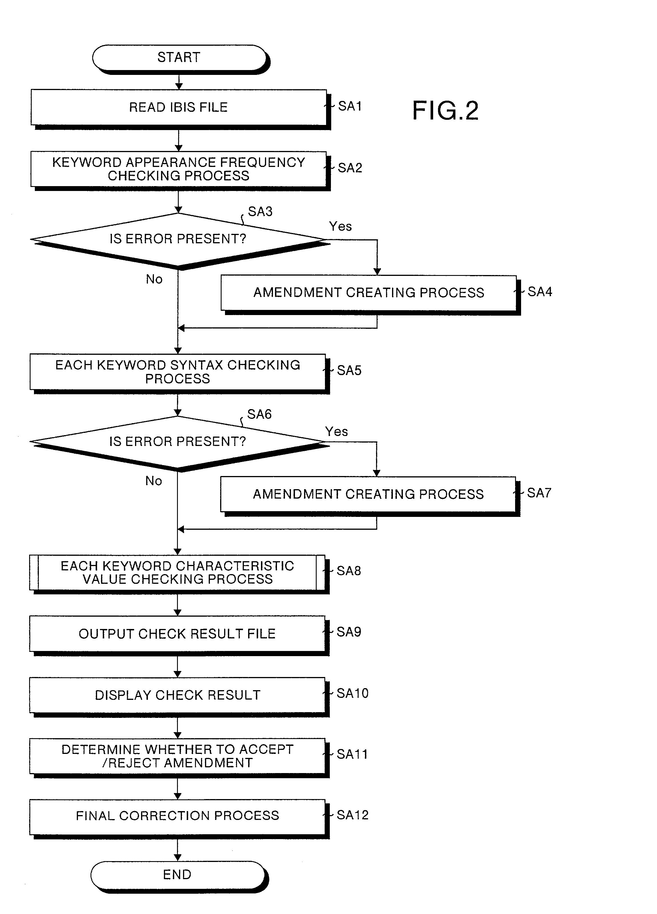
[0054]Embodiments of an automatic device model correcting program, an automatic device model correcting apparatus, and an automatic device model correcting method are described below in detail by referring to the accompanying drawings.

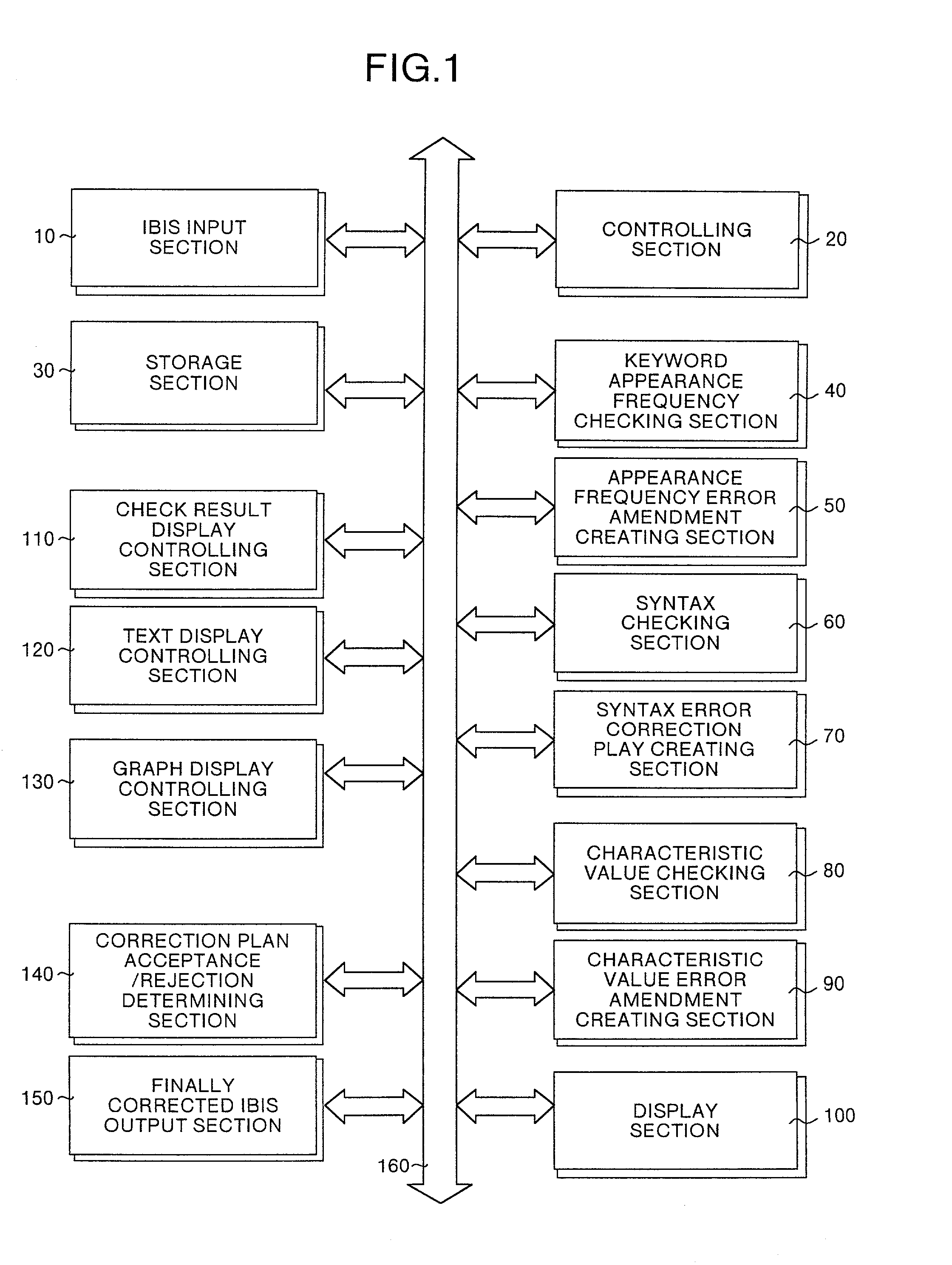
[0055]FIG. 1 is a block diagram showing a configuration of an embodiment of the present invention. FIG. 1 illustrates a configuration of an automatic device model correcting apparatus for executing an automatic device model correcting program and an automatic device model correcting method. The automatic device model correcting apparatus is provided for an electronic maker side.

[0056]As shown in FIG. 1, an IBIS input section 10 is used to input an IBIS file having a format same as that of the IBIS file F0 (refer to FIG. 29 and FIG. 30). The IBIS file is supplied from a semiconductor vendor to an electronic maker and serves as a file corresponding to the IBIS model. A controlling section 20 controls various sections of an automatic device model correcti...


PUM


Abstract

The apparatus comprises the syntax checking section that checks the syntax of a device model according to a check table showing the relation between the syntax of the device model showing electrical characteristics of a semiconductor device and an amendment when deviating from the syntax. The syntax error amendment creating section corrects the device model according to a corresponding amendment when a description deviating from the syntax is checked by the syntax checking section.

Description

FIELD OF THE INVENTION[0001]The present invention relates to a technology for checking and automatically correcting a device model used for a transmission simulation on a printed circuit board.BACKGROUND OF THE INVENTION[0002]Recently, each of many electronic makers receives a semiconductor device and a device model obtained by modeling the semiconductor device from a semiconductor vendor and performs circuit design and transmission simulation of a printed circuit board to be mounted on an electronic device. Moreover, though a spice model and an IBIS (Input / output Buffer Information Specification) model are publicly known as device models, the latter IBIS model is mainstream.[0003]Therefore, most electronic makers respectively perform circuit design and transmission simulation of a printed circuit board using a semiconductor device according to an IBIS model received from a semiconductor vendor. However, when checking by a semiconductor vendor is not strict, an IBIS model in which m...

Claims


Application Information

Patent Timeline
IPC IPC(8): G06F17/50H01L21/32H01L29/00
CPCG06F17/5036G06F30/367
Inventor TOSAKA, MASAKIKARINO, TOSHIOKOIZUMI, TATSUOYONEDA, JIRONAGATA, MEGUMIORIHARA, HIROYUKIKAWATA, HIKOYUKI
Owner FUJITSU LTD
Why Eureka
Try Eureka