Integrated circuit with improved signal noise isolation and method for improving signal noise isolation

a technology of integrated circuits and signal noise isolation, which is applied in the direction of semiconductor devices, semiconductor/solid-state device details, electrical apparatuses, etc., can solve the problems of affecting the performance of sensitive circuitry on the soc, unsatisfactory electrical interaction,

Active Publication Date: 2006-11-21
NORTH STAR INNOVATIONS
View PDF10 Cites 50 Cited by
  • Summary
  • Abstract
  • Description
  • Claims
  • Application Information

AI Technical Summary

Problems solved by technology

For example, a signal in one circuit may disrupt a signal in an adjacent circuit.
This undesirable electrical interaction may be referred to as noise and/or crosstalk that may occur due to...

Method used


Image

  • Integrated circuit with improved signal noise isolation and method for improving signal noise isolation
  • Integrated circuit with improved signal noise isolation and method for improving signal noise isolation
  • Integrated circuit with improved signal noise isolation and method for improving signal noise isolation

Examples


Embodiment Construction

[0009]The following detailed description is merely exemplary in nature and is not intended to limit the invention or the application and uses of the invention. Furthermore, there is no intention to be bound by any expressed or implied theory presented in the preceding technical field, background, or the following detailed description.

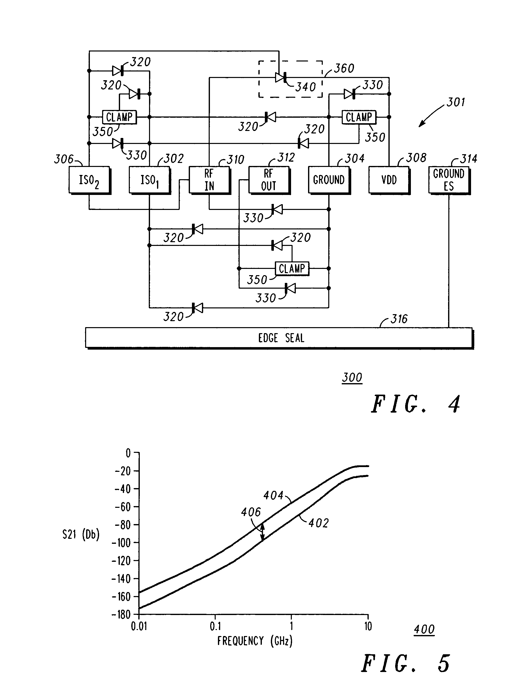
[0010]One embodiment of the present invention provides a method for minimizing substrate crosstalk between electrostatic discharge (ESD) protected pads, associated with circuit supply and ground lines, and a system-on-chip in a SOC system. An improved ESD protected pad design and structure that accomplishes that goal may apply to SOC designs that include RF, analog, and digital circuits where signal isolation is a major design criterion.

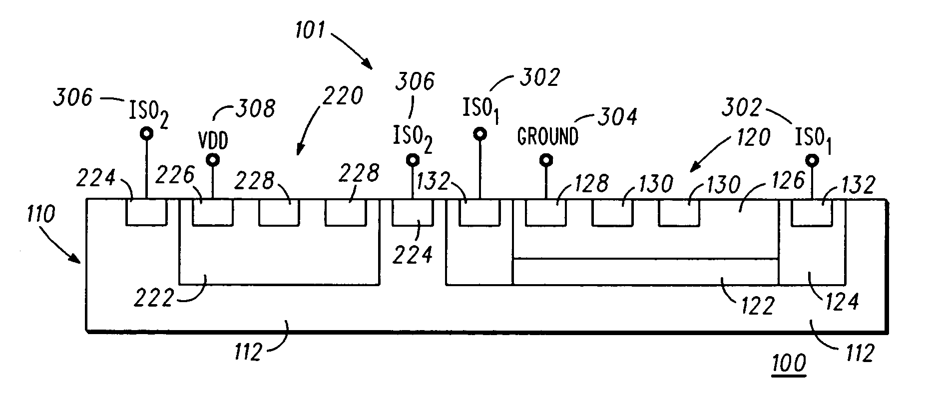
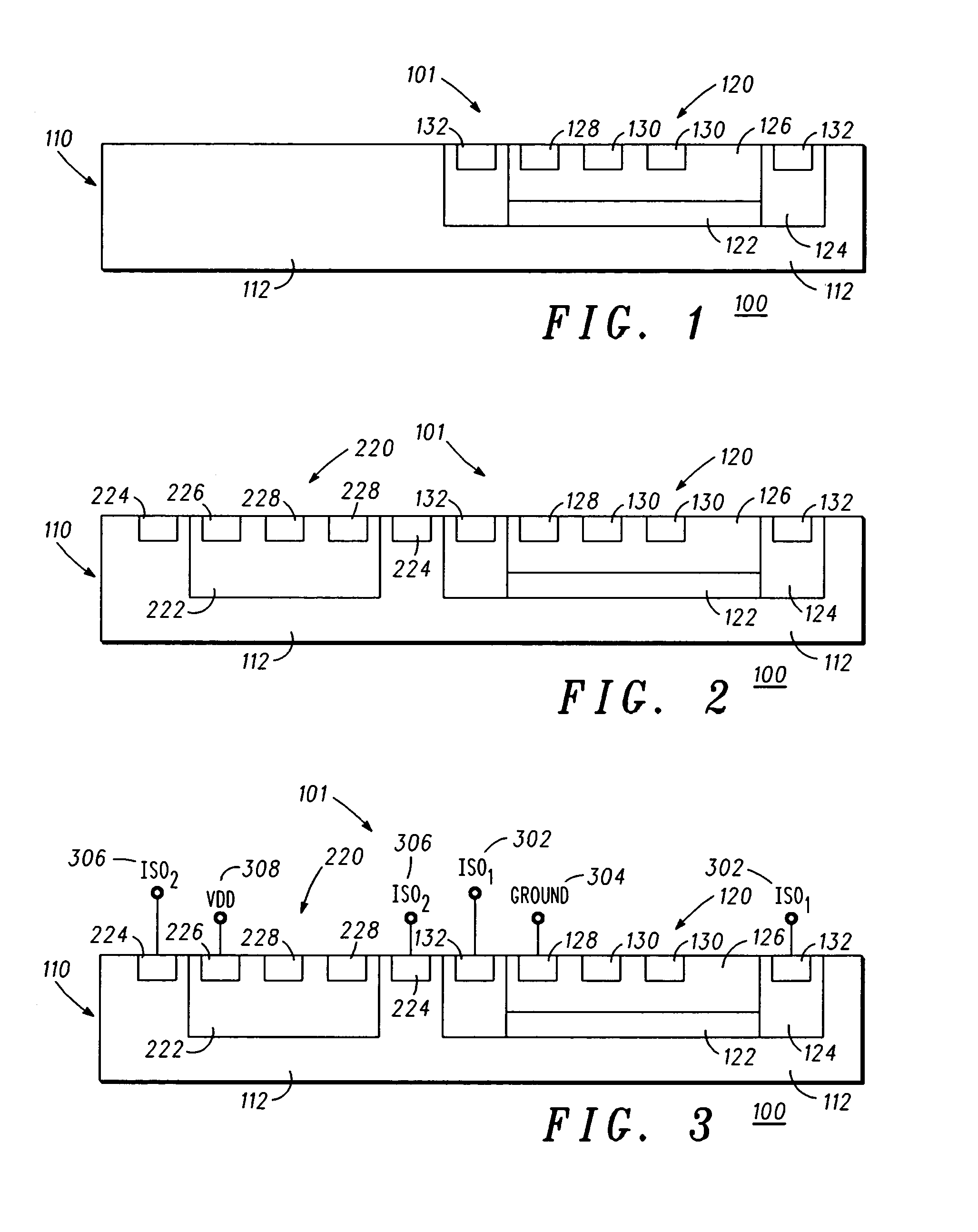
[0011]FIGS. 1–3 are cross-sectional views of a portion of a system-on-chip 100, including a mixed signal circuit, comprised of a NMOS device and a PMOS device, that together form a transceiver 101, as well as ESD protect...


PUM


Abstract

A system-on chip (SOC) (100) and method of isolating noise in a SOC, including a plurality of noise sensitive circuit blocks (120, 220) and ESD protected pads (302, 304, 306, 308, 310, 312, and 314). A VDD isolation pad (302) is connected to an N well ring (124) of the first noise sensitive circuit (120) to collect noise from the substrate (110) and isolate the circuit from the P well region (112). A ground protected pad (304) is connected to an isolated P well (126) of a first noise sensitive circuit (120). The ground pad (304) collects noise from the isolated P well (126) and sends it to ground. A dedicated ground isolation pad (306) is connected to a P well ring (224) of a second noise sensitive circuit (220). The dedicated ground isolation pad (306) collects noise from the P well ring (224) and sends it to ground. The dedicated ground isolation pad (306) and the ground pad (304) collect noise that would normally propagate between the first and second noise sensitive circuits (120, 220) and additional circuits that share the same substrate (110).

Description

FIELD OF THE INVENTION[0001]This present invention generally relates to the field of integrated circuits and more particularly, to improving substrate noise isolation and crosstalk in system-on-chip (SOC) applications.BACKGROUND OF THE INVENTION[0002]Microelectronic chip integration technology has lead to recent improvements. In the past, electronic systems have required the use of multi-chip systems including many microchips and discrete components. However, as integrated circuit technology has advanced, systems-on-chip (SOCs) have become more popular. A single SOC may contain, for example, numerous digital and analog integrated circuit components, e.g. CPUs, memories, random logic, RF circuitry, etc. Circuits of the type described above (i.e. mixed signal circuits that integrate various digital and analog circuit blocks on an SOC) present certain challenges. For example, a signal in one circuit may disrupt a signal in an adjacent circuit. This undesirable electrical interaction ma...

Claims


Application Information

Patent Timeline
IPC IPC(8): H01L29/76
CPCH01L23/552H01L27/0248H01L2924/0002H01L2924/00
Inventor BANERJEE, SUMAN K.FERRER, ENRIQUEHARTIN, OLIN L.SECAREANU, RADU M.
Owner NORTH STAR INNOVATIONS
Why Eureka
Try Eureka