Programmable phase shift and duty cycle correction circuit and method

a phase shift and duty cycle correction technology, applied in the field of electronic circuits, can solve problems such as significant impact on system performance and/or reliability, one or more system components, and design and operation problems of electronic systems

Active Publication Date: 2006-11-21
CYPRESS SEMICON CORP
View PDF13 Cites 85 Cited by
  • Summary
  • Abstract
  • Description
  • Claims
  • Application Information

AI Technical Summary

Benefits of technology

This patent describes a system for generating an output signal based on two input signals. It includes various components like delays, storages, charging circuits, etc., along with configurable settings that determine its behavior. By adjusting these settings, it becomes possible to change things like the duty cycle and phase relationship between the input and output signals. Additionally, there's a programmable digital-to-analog converter that allows for precise customization of the reference voltage levels. Overall, this technology provides flexibility and precision in shaping the desired output waveform.

Problems solved by technology

This patent discusses how timeows and unstable factors like clock skew and jitter impact the performance and reliability of synchronous systems. Clock skew refers to the misalignment of clock signals and data signals, causing errors in the transmission process. Jitter describes the deviation of data arrival times caused by changes in latency. These challenges make it difficult to design reliable circuits and meet specific timing requirements. Existing solutions use various methods including phased lock loops and delayed lines to address these concerns, but they come with their own limitations. There is also no way to modify the duty cycle of the output signal without introducing new difficulties. Thus, there is a technical problem of providing an improved phase shift and duty cycle correction circuit and method that overcomes the shortcomings of existing solutions.

Method used


Image

  • Programmable phase shift and duty cycle correction circuit and method
  • Programmable phase shift and duty cycle correction circuit and method
  • Programmable phase shift and duty cycle correction circuit and method

Examples


Embodiment Construction

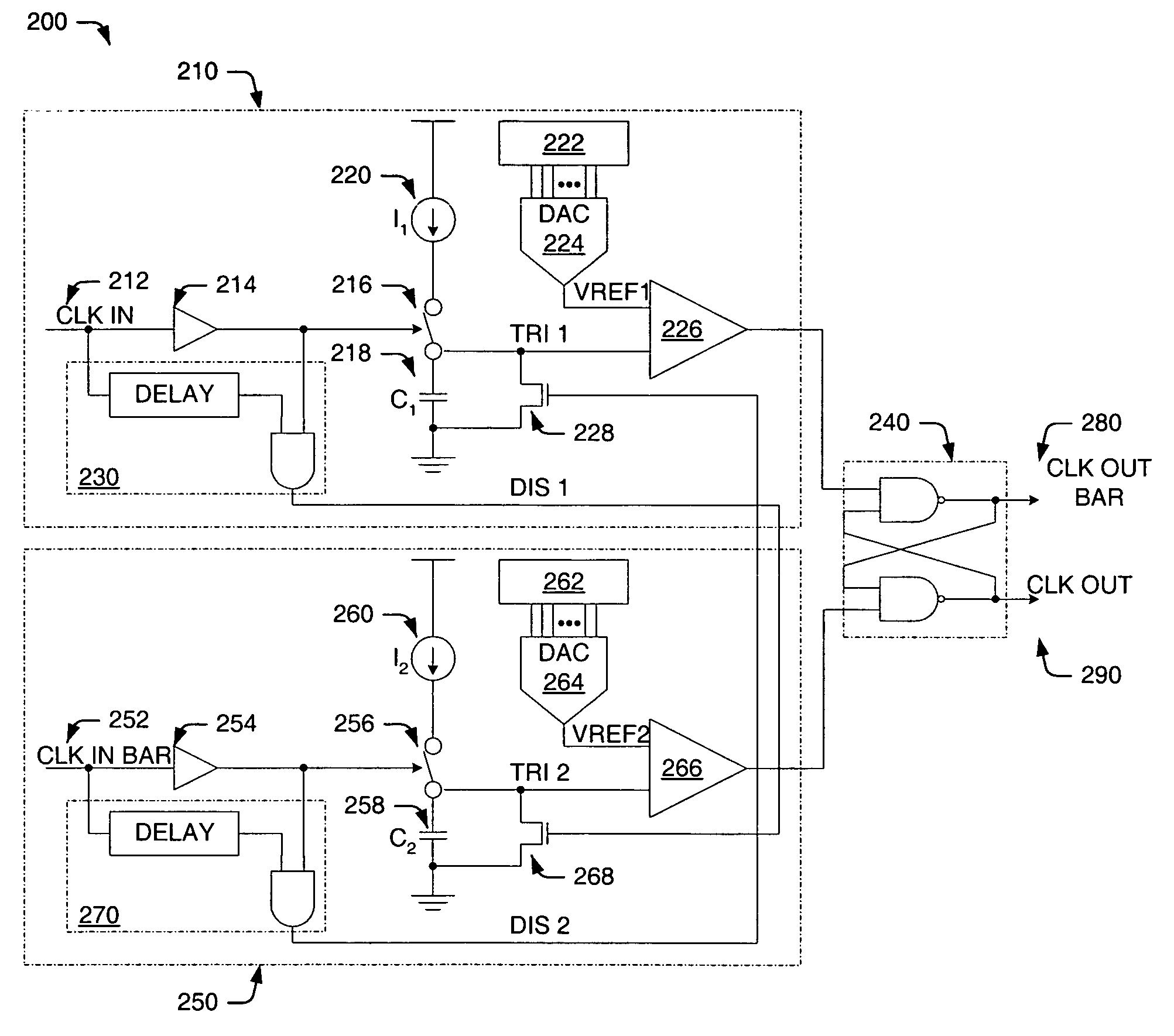
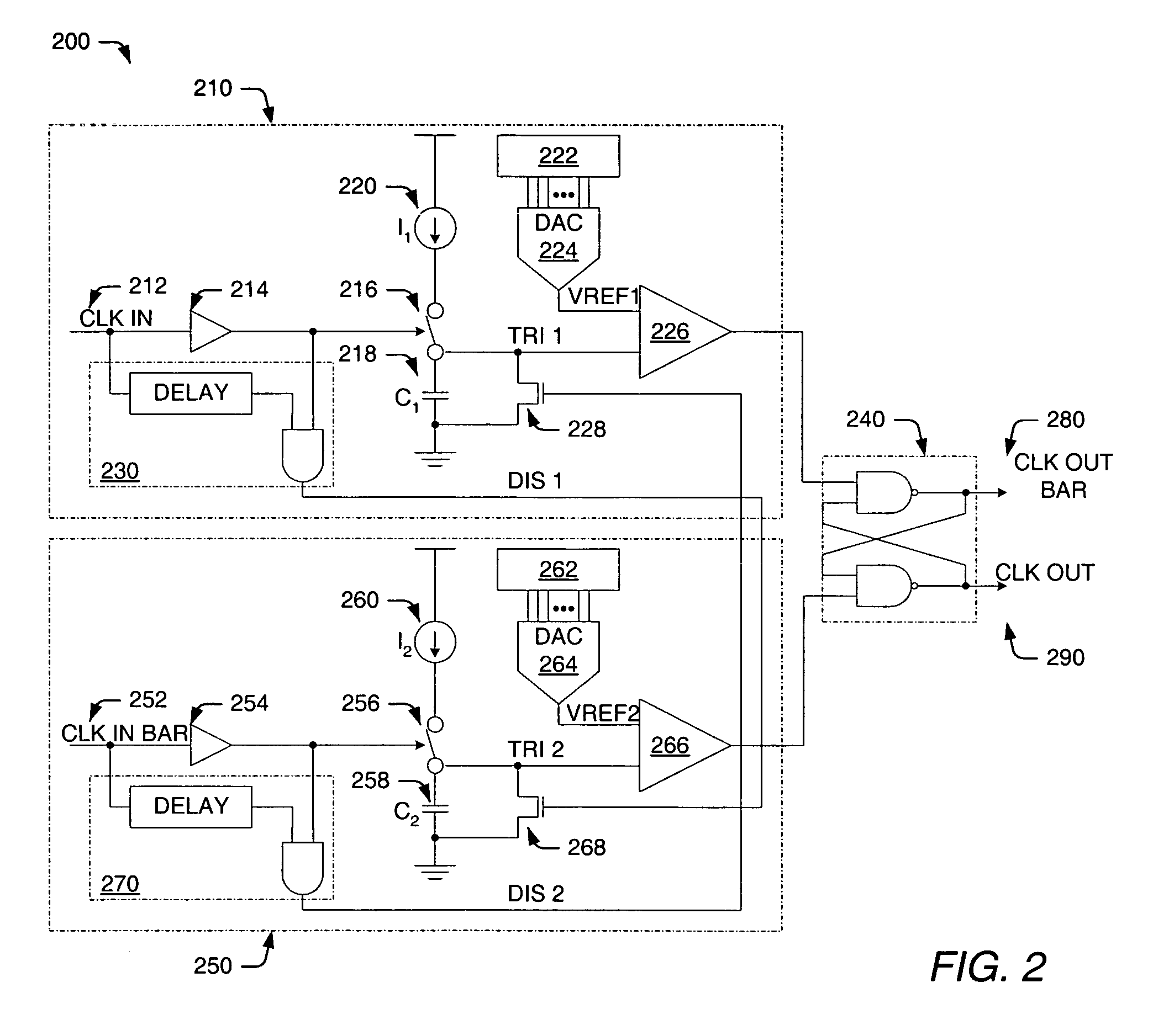
[0033]An embodiment of an improved phase shift and duty cycle correction circuit is shown in FIG. 2. In general, the improved circuit enables both rising and falling edges of a generated clock signal to be shifted in time by an independently programmable amount. In some embodiments, the programmable amounts may be set by a manufacturer or end-user of the circuit; however, additional circuit components may be provided, in other cases, for detecting and automatically setting an appropriate phase shift amount. By shifting the rising and falling edges of the clock signal, the improved circuit provides a unique means for correcting, or otherwise modifying, a duty cycle of the generated clock signal. In one embodiment, means for adjusting the phase and duty cycle of the generated clock signal may be implemented with a simple digital-to-analog converter (DAC), programmable by a variety of methods, including but not limited to, register bits, hardwired bits, externally supplied inputs, prog...


PUM


Abstract

A phase shift and duty cycle correction circuit is disclosed herein as comprising a programmable digital to analog converter (DAC), a storage device (e.g., a capacitor), a charge sub-circuit and dump sub-circuit for charging and discharging the storage device, respectively, a comparator, and a clock driver circuit. A linearly increasing (or ramped) voltage waveform is generated within the storage device by the charging and discharging actions of the charge and dump sub-circuits; a periodic process which is controlled by opposite phases of the input clock. By programming the DAC control input to change the slicing threshold of the ramped waveform, the circuit and method described herein provides a means for programmable phase shifting and duty cycle correction.

Description


Claims


Application Information

Patent Timeline
Owner CYPRESS SEMICON CORP
Why Eureka
Try Eureka