
Radiation hardening of logic circuitry using a cross enabled, interlocked logic system and method

a logic system and logic technology, applied in logic circuits, pulse techniques, reliability increasing modifications, etc., can solve the problems of large amount of radiation exposure of integrated circuits, large amount of disruption of terrestrial-based devices that use integrated circuits, and high density of integrated circuits

Active Publication Date: 2006-11-28
HONEYWELL INT INC
View PDF6 Cites 18 Cited by
  • Summary
  • Abstract
  • Description
  • Claims
  • Application Information

AI Technical Summary

Benefits of technology

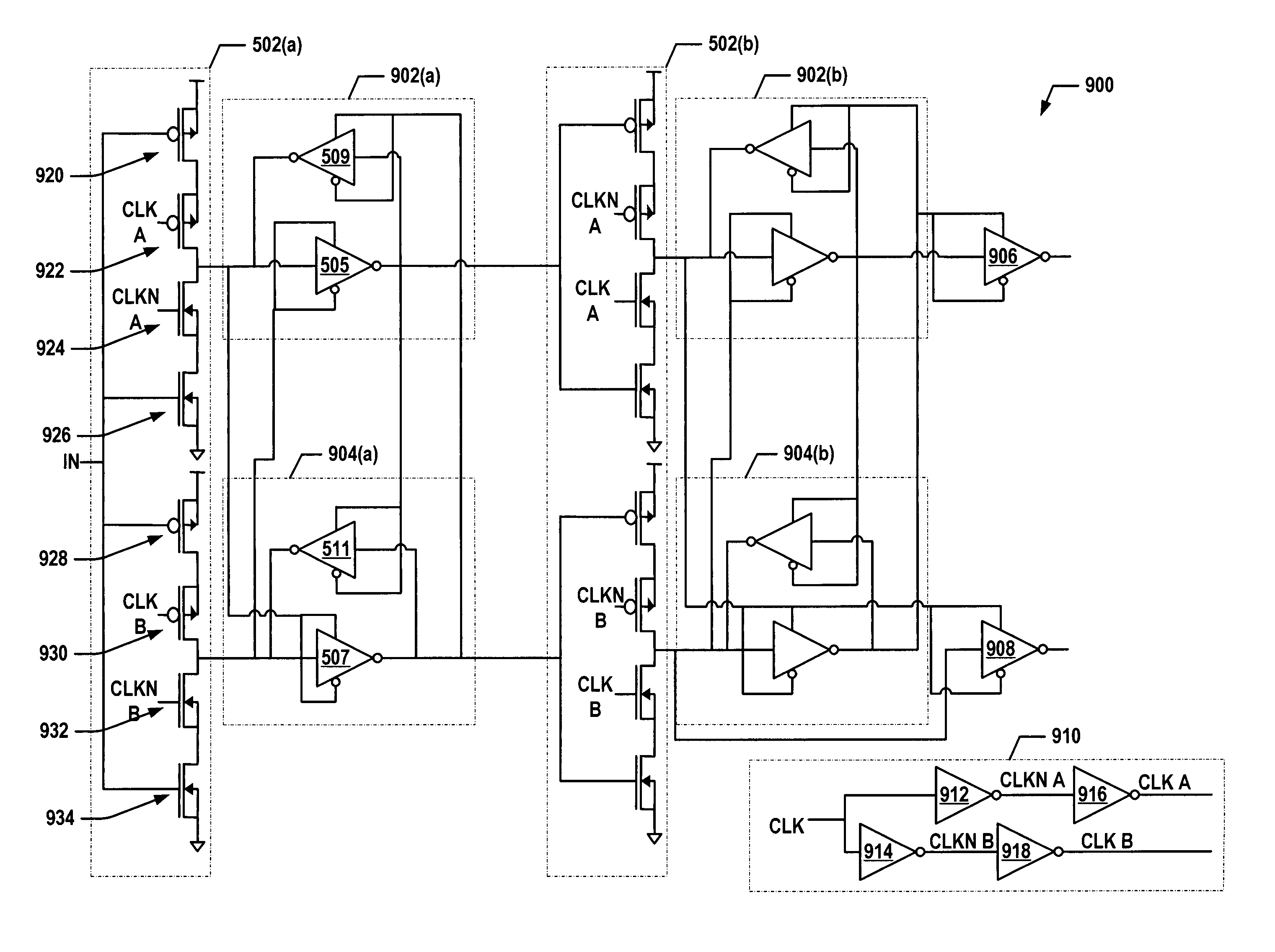
The patent describes a system and method for making a logic circuit more robust against single-event upsets and transients. The system includes a logic circuit, two feed-forward devices, and two feedback devices. The logic circuit produces two redundant signals that are independently obtained. The feed-forward devices receive both redundant signals and produce a feed-forward signal if they are in an expected state. The feedback devices receive both feed-forward signals and feed them back to the redundant signals to complete feedback loops. This system can prevent the effects of radiation particles from causing unexpected changes in the logic circuit.

Problems solved by technology

Along with these necessities, space, weight and cost limitations generally cause these integrated circuits be very densely populated and highly complex.
As a consequence of operating in intergalactic space, earth orbital space, and high atmospheric altitudes, however, the integrated circuits are exposed to a large amount of radiation, which can effect their operation and, in turn, their reliability.
Recently, however, several radiation-laden atmospheric storms, which emanated from a coronal mass ejection of the sun, expanded into space, penetrated the Earth's magnetic field and disrupted a significant amount of terrestrial-based devices that use integrated circuits.
When a radiation particle interferes with an integrated circuit, it can slow the circuit's performance and even upset circuit operation.
In Very Large Scale Integration (VLSI) circuits, radiation particles can also generate significant transient voltage and current disturbances on internal supply networks (e.g. power and ground nodes).
A radiation particle that passes into and through an integrated-circuit device transfers energy from the particle into the material surrounding the region into which the particle strikes or “hits.” This energy transfer creates undesirable hole-electron pairs in the surrounding region.
As a result, the particle can only create a finite amount of charge per unit distance over the length of its track.
The consequence of having a temporary voltage disturbance on the transistor node, however, may be problematic because the SET condition may be propagated through the larger system.
If the particle strike is outside the sensitive volume, the created charge may not be able to get to the critical node to cause a SEE condition.
In this case, the particle strike may not create an immediate state change, but it can delay a desired state change from occurring.
In addition to causing undesirable state changes, the created hole-electron concentrations can be quite high, e.g., much higher than the surrounding structure of the semiconductor device, i.e., higher than the N or P-type impurity concentrations.
This may result in a switching lifetime that is temporarily much shorter than normally present in the structure of the semiconductor device.
As can be readily discerned from above, modern integrated circuits are susceptible to SEE conditions.
These solutions typically are not area efficient.
However, if one or both of the first and second redundant signals are in an unexpected state due to, for example, a radiation-particle intrusion, then one or both of the first and second feed-forward devices do not provide its respective feed-forward signal.

Method used


Image

  • Radiation hardening of logic circuitry using a cross enabled, interlocked logic system and method
  • Radiation hardening of logic circuitry using a cross enabled, interlocked logic system and method
  • Radiation hardening of logic circuitry using a cross enabled, interlocked logic system and method

Examples


Embodiment Construction

Overview

[0057]FIG. 4 is a block diagram illustrating exemplary architecture of a cross-enabled, interlocked logic system 400 for hardening a logic circuit against single-event upset (SEU) and / or single-event transient (SET) conditions in accordance with an exemplary embodiment. This cross-enabled, interlocked logic system 400 may be deployed with logic circuitry 402 that provides independently-obtained redundant signals. The construction (e.g., transistor-level fabrication and configuration) of the logic circuitry 402 may provide a first level of hardening against SEU and / or SET conditions.

[0058]The cross-enabled, interlocked logic system 400 may also be deployed with first and second feed-forward modules 404, 406 and first and second feedback modules 408, 110. By their construction and intercoupling (i.e., the manner in which the modules are coupled together), the first and second feed-forward modules 404, 406 and feedback modules 408, 410 provide not only the first level, but also...


PUM


Abstract

A system and method for hardening a logic circuit against radiation-event effects is provided. The system may include a logic circuit, first and second feed-forward devices, and first and second feedback devices. The logic circuit may be operable to output independently-obtained first and second redundant signals responsive to a desired input signal. Each of the first and second feed-forward devices may receive both of the first and second redundant signals. When the first and second redundant signals are in expected states, then the first and second feed-forward devices may responsively provide respective first and second feed-forward signals. Each of the first and second feedback devices may receive both of the first and second feed-forward signals. When the first and second feed-forward signals are in expected states, then the first and second feedback devices responsively feed respective first and second feedback signals back to the respective first and second redundant signals.

Description

BACKGROUND[0001]1. Field[0002]The following relates to microelectronic circuits, and more particularly, to single-event effect (“SEE”) resistant or hardened circuits.[0003]2. Related Art[0004]Integrated circuits used in devices that operate in intergalactic space, earth orbital space, and high atmospheric altitudes (e.g., commercial flight altitudes) generally have to be highly reliable and operate using very low levels of power. Along with these necessities, space, weight and cost limitations generally cause these integrated circuits be very densely populated and highly complex.[0005]As a consequence of operating in intergalactic space, earth orbital space, and high atmospheric altitudes, however, the integrated circuits are exposed to a large amount of radiation, which can effect their operation and, in turn, their reliability. Because the Earth's magnetic field deflects most outer space radiation, terrestrial-based integrated circuits are not normally exposed to large amounts of ...

Claims


Application Information

Patent Timeline
Patent Type & Authority Patents(United States)
IPC IPC(8): H03K19/007H03K19/003
CPCH03K19/00338
Inventor CALRSON, ROY M
Owner HONEYWELL INT INC
Learn More