Memory device including barrier layer for improved switching speed and data retention

a memory device and barrier layer technology, applied in the field of memory devices, can solve the problems of volatile memory devices losing their information, increasing the volume, use and complexity of computers and electronic devices, and increasing the complexity of computing and electronic devices

Active Publication Date: 2006-12-26
VALLEY DEVICE MANAGEMENT
View PDF5 Cites 20 Cited by
  • Summary
  • Abstract
  • Description
  • Claims
  • Application Information

AI Technical Summary

Problems solved by technology

The volume, use and complexity of computers and electronic devices are continually increasing.
The long term storage mediums typically store larger amounts of information at a lower cost, but are slower than other types of storage devices.
Volatile memory devices generally lose their information if they lose power and typically require periodic refresh cycles to maintain their information.
However, silicon-based devices are approaching their fundamental physical size limits.
Inorganic solid state devices are generally encumbered with a complex architecture which leads to high cost and a loss of data storage density.
The volatile semiconductor memories based on inorganic semiconductor material must constantly be supplied with electric current with a resulting heating and high electric power consumption in order to maintain stored information.
Non-volatile semiconductor devices have a reduced data rate and relatively high power consumption and large degree of complexity.
Typically, fabrication processes for such cells are also not reliable.

Method used


Image

  • Memory device including barrier layer for improved switching speed and data retention
  • Memory device including barrier layer for improved switching speed and data retention
  • Memory device including barrier layer for improved switching speed and data retention

Examples


Embodiment Construction

[0022]Reference is now made in detail to a specific embodiment of the present invention which illustrates the best mode presently contemplated by the inventors for practicing the invention.

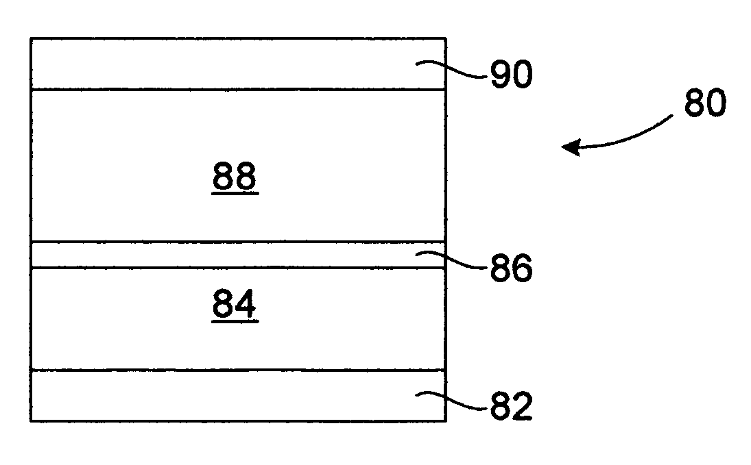
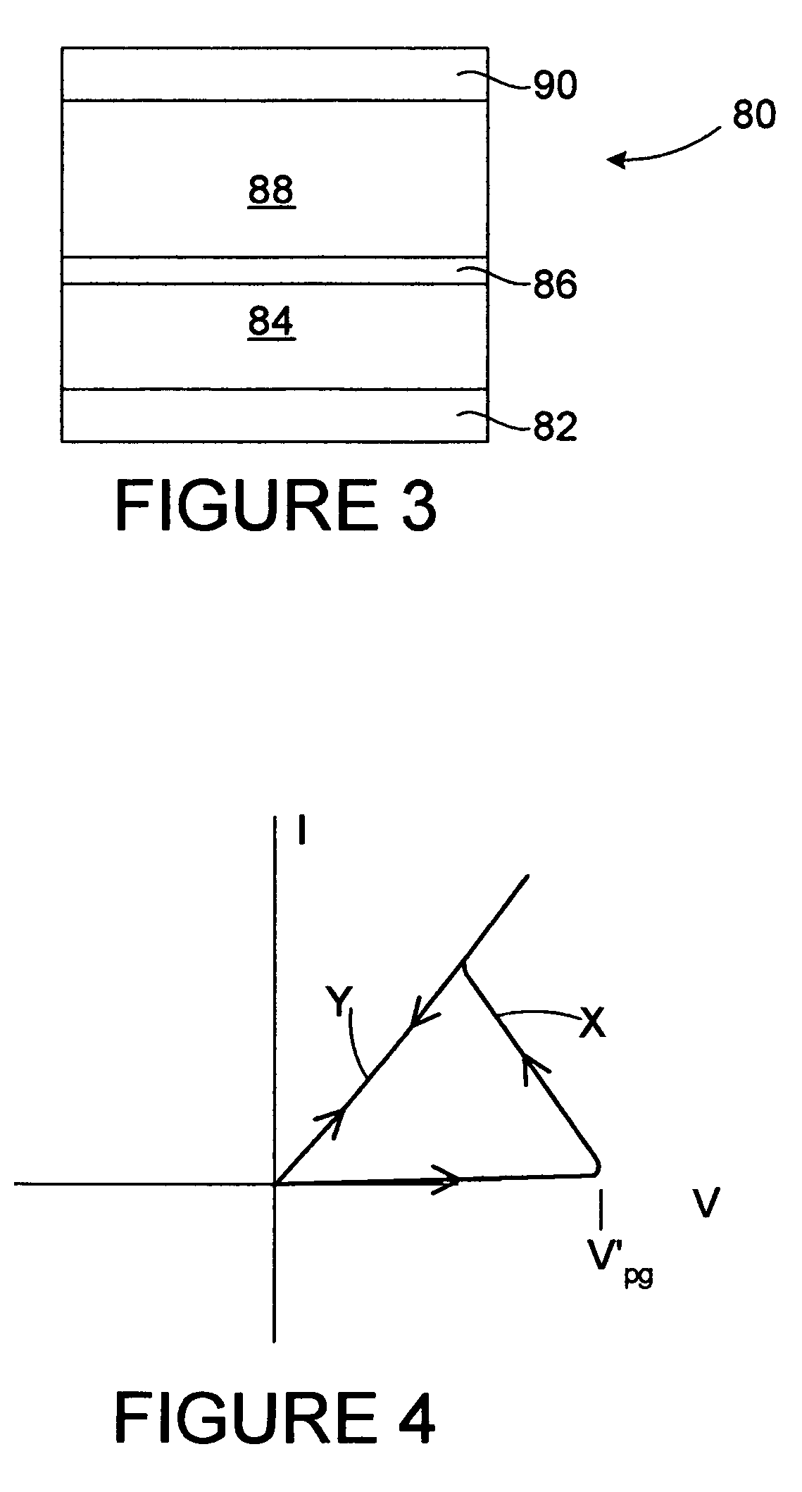
[0023]FIG. 3 illustrates an embodiment of memory device 80 of the present invention. The memory device 80 includes a Cu electrode 82, a copper sulfide passive layer 84 on, over and in contact with the electrode 82, a barrier layer 86 (which may for example be CuOx, WOx, NiOx, or TiOx, formed by for example deposition or oxidation) on, over and in contact with the copper sulfide layer 84, an active layer 88 (which may for example be an inorganic layer such as Cu2O or various organic polymers) on, over and in contact with the barrier layer 86, and a Ti electrode 90 on, over and in contact with the active layer 88.

[0024]Initially, assuming that the memory device 80 is unprogrammed, in order to program the memory device 80, an increasingly negative voltage is applied to the electrode 90, while the ele...


PUM


Abstract

The present memory device includes a first electrode, a passive layer on and in contact with the first electrode, the passive layer including copper sulfide, a barrier layer on and in contact with the passive layer, an active layer on and in contact with the barrier layer, and a second electrode on and in contact with the active layer. The inclusion of the barrier layer in this environment increases switching speed of the memory device, while also improving data retention thereof.

Description

BACKGROUND OF THE INVENTION[0001]1. Technical Field[0002]This invention relates generally to memory devices, and more particularly, to a memory device with improved switching speed and data retention.[0003]2. Background Art[0004]The volume, use and complexity of computers and electronic devices are continually increasing. Computers consistently become more powerful, new and improved electronic devices are continually developed (e.g., digital audio players, video players). Additionally, the growth and use of digital media (e.g., digital audio, video, images, and the like) have further pushed development of these devices. Such growth and development has vastly increased the amount of information desired / required to be stored and maintained for computer and electronic devices.[0005]Generally, information is stored and maintained in one or more of a number of types of storage devices. Storage devices include long term storage mediums such as, for example, hard disk drives, compact disk ...

Claims


Application Information

Patent Timeline
Patent Type & Authority Patents(United States)
IPC IPC(8): G11C11/00
CPCG11C13/0009G11C13/0014G11C13/0016H01L45/12H01L45/085H01L45/1233H01L45/146G11C2213/51H10N70/245H10N70/801H10N70/826H10N70/8833
Inventor KRIEGER, JURISPITZER, STUART
Owner VALLEY DEVICE MANAGEMENT
Why Eureka
Try Eureka